October 30th, 2014 ~ by admin
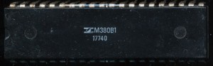
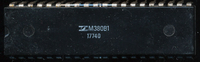
SGS-Ates M380B1 – 1977
In the 1970’s the computer age was booming. New processor designs were being pushed out by the month, and computers to use them were being designed and outdated just as fast. Not all markets were growing as fast as the American market, or could support the newest, most complex, and expensive designs. Thus, it was common for semiconductor companies to design chips specifically for these markets. Europe was considered one of these markets, where simpler more affordable devices were easier to sell, thus CPUs were made specifically for the European market. Many of these designs are still nearly impossible to find outside of Europe.
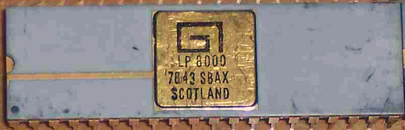
General Instruments was one such company. Their premier processor, the CP1600, was a 16-bit deign based on the PDP-11. It was one of the first NMOS 16-bit processors (along with the TI9900) and was released in 1975. GI also had the PIC line of 8-bit MCUs for control oriented tasks, which is still in production today. GI wanted a design for the European market so in 1976 released the LP8000, LP for Logic Processor. The LP8000 was a 3-chip simple processor and cost a mere $10. It could execute 48 instructions (including ADD, but subtraction was not supported directly) at a clock speed of 800 kHz and was made on a PMOS process. The chipset consisted of the LP8000 processor which contained the ALU and 48 8-bit registers as well as the accumulator a 6-bit address bus and 8-bit of I/O. Combining the 6-bit address and 8-bit I/O busses allowed the LP8000 to directly address 16K of memory. The 11-bit Program Counter was contained off chip, on the LP6000 which also contained an additional 16 lines of I/O and 1K of ROM for program storage. Clock generation was provided by the LP1030 and memory expansion was handled by the LP1000 (which also includes a 11-bit PC for interfacing up to 2K of memory) while the LP1010 handled I/O expansion. In order to be successful in Europe GI needed to find a European partner who could make, market and sell the design.

GI LP8000
That partner ended up being SGS-Ates of Italy (which later would become ST Microelectronics). SGS-Ates second sourced the LP8000 as the M38 (or M380) series. The M380 was the processor element, while the M382 was the 1K ROM equivalent of the LP6000. In addition SGS-Ates made the M381 which had 18 bytes of RAM and 768 bytes of ROM as well as the PC. Like the LP8000 the M380 drew about 1 Watt of power and required a +5V and -12V supply (or a -5V and -17V). The M380 was rather short lived as SGS-Ates soon licensed the Zilog Z80 which was a much more powerful, yet still inexpensive, design. When SGS-Ates purchased Mostek from United Technologies they added yet another 8-bit design, the F8, which Mostek had licensed from Fairchild. These processors quickly replaced the M380/LP8000 and with no market, it faded into obscurity.
October 11th, 2014 ~ by admin
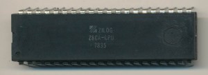
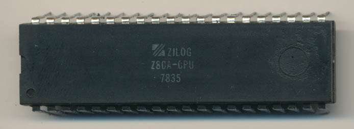
Zilog Z80A CPU -1978
Ken Shirriff has an excellent write up about the Zilog Z80 and why its pin-out, specifically the Data lines, is a bit convoluted. Rather then being in order (such as D0-D7) the original Z80 is D4,D3.D5,D6,D2,D7,D0,D. Its functional but its not pretty and can lead to some interesting PCB layout issues. Ken uses data/imaging from the Visual6502 project to look at the on die reasons for this. Essentially it came down to saving die space. there literally was not enough room to route the data connections within the confines of the die size. Keeping the die size small allowed Zilog, and its many second sources), to keep prices down. In the early days Zilog contracted Mostek to make much of their processors, so die size and the associated cost were a big issue.
January 17th, 2014 ~ by admin
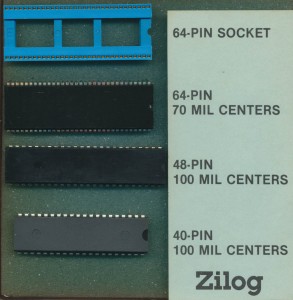
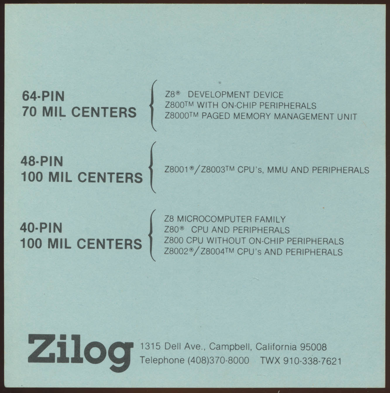
Zilog Packages available in 1985
Last week we showed you an educational kit from Zilog showing the process involved in making and assembling a Z80 processor, from polished wafer to packaging. Zilog also made a kit for marketing the various packages used. This kit contains a shrink DIP 64 pin socket, a shrink DIP 64pin package, a 48 pin DIP and 40 pin DIP, all the common packages used at the time.
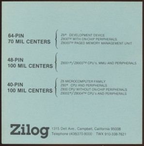
Zilog Packages – Z8 Z80 Z800 and Z8000
At the time is a little hard to track down as no date is provided with this kit. We can get very close though looking at the back where Zilog lists which devices are available in these packages. The usual Z80 and Z8000 series are both there as well as the Z8 microcontroller family. The one odd-ball is the Zilog Z800. The Z800 was an upgraded Z80 released in 1985, adding on chip cache an MMU and a vastly expanded instruction set (over 2000 instruction/addressing modes). It was wholly unsuccessful partly do to bad marketing by Zilog, and partly because it did more then it needed to. It never entered mass production, and by 1986 Zilog has redesigned it, converted the design to CMOS (from NMOS) and released it as the Z280 which met the same fate as the Z800. It seemed that making an overly complicated Z80 wasn’t what the market wanted. THe Z180 (designed by Hitachi) and the Zilog eZ80 (released in 2001), have enjoyed much wider success, mainly because they kept closer to the simplicity of the original Z80.
So when was this kit put together? Likely 1985, as the Z800 was nly talked about for a few months before quietly being put away.
January 9th, 2014 ~ by admin
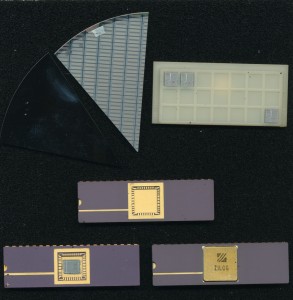
Zilog Z-80 Kit – Click for full size
Here is a neat kit from Zilog. Its an Educational Kit showing some of the steps of producing a Z-80 processor. It includes:
- A raw polished wafer slice before any etching has occured. This is what a processor starts out with (sliced from a single large ingot)
- A slice of an etched wafer. In this case it appears to be some sort of memory, but the process is the same for a processor.
- Several cut die, these are cut from a wafer after testing. The red dot notes that these particular dice failed one or more of the tested and should be discard. Thats probably why they made it into this kit rather then a saleable device.
- An bare unfinished package. These packages are rarely if ever made by the company making the processor. They are made by companies such as NGK (who also makes spark plugs) and Kyocera. The bottom of the die cavity is usually connected to the ground pin of the package.
- Next is a package with the die placed in the die cavity. No bonding wires are installed in this example but that would be the next step. The very fine gold bonding wires connect the pad ring on the edge of the die, to the pads in the die cavity. Those [ads are connected through the package to the 40 pins of the ceramic DIP package.
- Finally we have a completed device. The lid is usually soldered or brazed onto the package and markings applied. The marking on this example make it a ‘Marketing Sample’ as they are there solely for looks, rather then to identify the device, its date, and lot.
These types of kits were produced for educational use, and given to schools, as well as sales people to assist in marketing Zilog’s various products
October 15th, 2010 ~ by admin
 In 1974 Federico Faggin left Intel after working on the 8-bit 8080 processor. He formed a company called ZiLOG and developed a much improved version of the 8080 called the Z80. It was released in 1976 after only 18 months of design. The Z80 was faster, cheaper, and simpler to build around then the 8080 and enjoyed extremely wide use. ZiLOG designed the CPU but it was marketed differently than most at the time. Any company could purchase a license to the design, and build them royalty free. They were also free to do with the design as they pleased. This resulted in dozens of companies making clones/versions of it. The Soviets made unlicensed copies as well. In fact other companies made more Z80s then ZiLOG did themselves.

Zilog Z-80 CPU 8400X CS – 1979 2.5MHz
The Z80 was not the only processor that ZiLOG made. Some of the processors/part numbering can be a bit confusing so we’ll look at each family and part that Zilog made up through 1985. After 1985 CMOS designs came out as well as dozens of variations. We just want to look at the first ten years of ZiLOG.

Zilog Z8300-3PS – 1984 2.5MHz
The Z80 itself was, of course, similar to the 8080 but single voltage, and only required a single clock phase. It was available in speeds of 2.5-8MHz. ZiLOG also made a low-power version known as the Z80L (Z8300) that ran from 1-2.5MHz. That’s really all there was to the Z80 family up through 1985.
Read More »