
Zilog Educational Sample Kit
Zilog Z-80 Kit – Click for full size
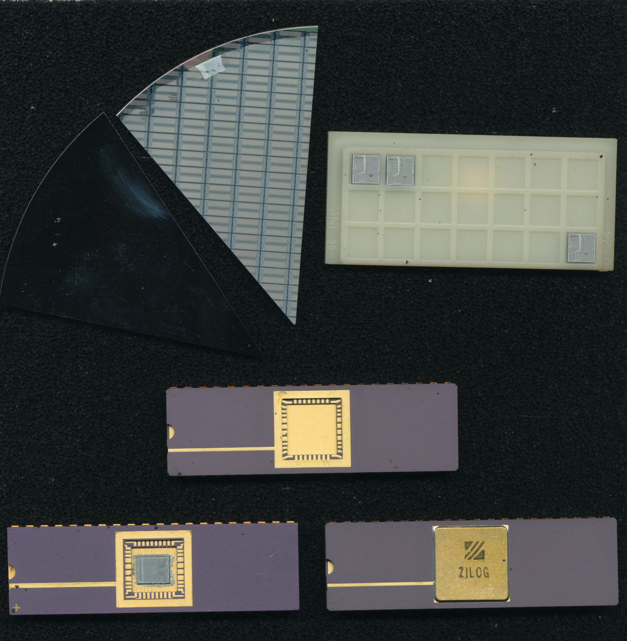
Here is a neat kit from Zilog. Its an Educational Kit showing some of the steps of producing a Z-80 processor. It includes:
- A raw polished wafer slice before any etching has occured. This is what a processor starts out with (sliced from a single large ingot)
- A slice of an etched wafer. In this case it appears to be some sort of memory, but the process is the same for a processor.
- Several cut die, these are cut from a wafer after testing. The red dot notes that these particular dice failed one or more of the tested and should be discard. Thats probably why they made it into this kit rather then a saleable device.
- An bare unfinished package. These packages are rarely if ever made by the company making the processor. They are made by companies such as NGK (who also makes spark plugs) and Kyocera. The bottom of the die cavity is usually connected to the ground pin of the package.
- Next is a package with the die placed in the die cavity. No bonding wires are installed in this example but that would be the next step. The very fine gold bonding wires connect the pad ring on the edge of the die, to the pads in the die cavity. Those [ads are connected through the package to the 40 pins of the ceramic DIP package.
- Finally we have a completed device. The lid is usually soldered or brazed onto the package and markings applied. The marking on this example make it a ‘Marketing Sample’ as they are there solely for looks, rather then to identify the device, its date, and lot.
These types of kits were produced for educational use, and given to schools, as well as sales people to assist in marketing Zilog’s various products
Posted in:
CPU of the Day