
Why the Zilog Z-80’s data pins are scrambled
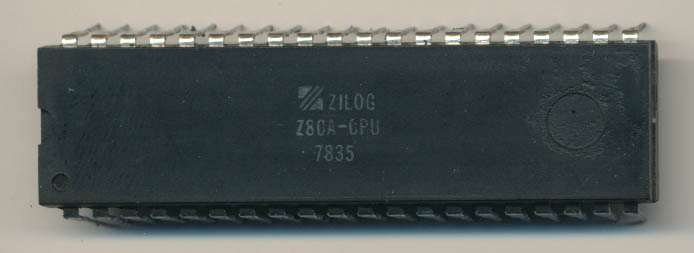
Zilog Z80A CPU -1978
Ken Shirriff has an excellent write up about the Zilog Z80 and why its pin-out, specifically the Data lines, is a bit convoluted. Rather then being in order (such as D0-D7) the original Z80 is D4,D3.D5,D6,D2,D7,D0,D. Its functional but its not pretty and can lead to some interesting PCB layout issues. Ken uses data/imaging from the Visual6502 project to look at the on die reasons for this. Essentially it came down to saving die space. there literally was not enough room to route the data connections within the confines of the die size. Keeping the die size small allowed Zilog, and its many second sources), to keep prices down. In the early days Zilog contracted Mostek to make much of their processors, so die size and the associated cost were a big issue.