Soviet’s First Planar Integrated Circuits
“Copy It”
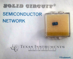
“Around the same time that Nikita Khrushchev declared his support for building Zelenograd. A Soviet student named Boris Malin returned from a year studying in Pennsylvania with a small device in his luggage – a Texas Instruments SN-51, one first integrated circuits sold in the United States. A thin man with dark hair and deep-set eyes, Malin was one of the Soviet Union leading experts on semiconductor devices. He saw himself as a scientist, not a spy. Yet Alexander Shokin, the bureaucrat in charge of Soviet microelectronics, believed the SN-51 was a device the Soviet Union must acquire by any means necessary. Shokin called Malin and a group of other engineers into his office, placed the chip under his microscope, and peered through the lens. «Copy it», he ordered them, «one-for-one», without any deviations. I’ll give you three months.“
Chris Miller
Chip War: The Fight for World’s Most Critical Technology. Chapter 8
In 1961, Fairchild Semiconductor patented integrated circuit fabrication technology that revolutionized the electronics industry. The central idea of this technology, called planar (in mathematics, “planarity” means a geometric image that can be drawn on a plane without intersecting lines) is that the design of an integrated circuit is initially represented as a set of drawings. These patterns are then sequentially “translated” onto a semiconductor material crystal using various physical and chemical processes (photolithography etc).
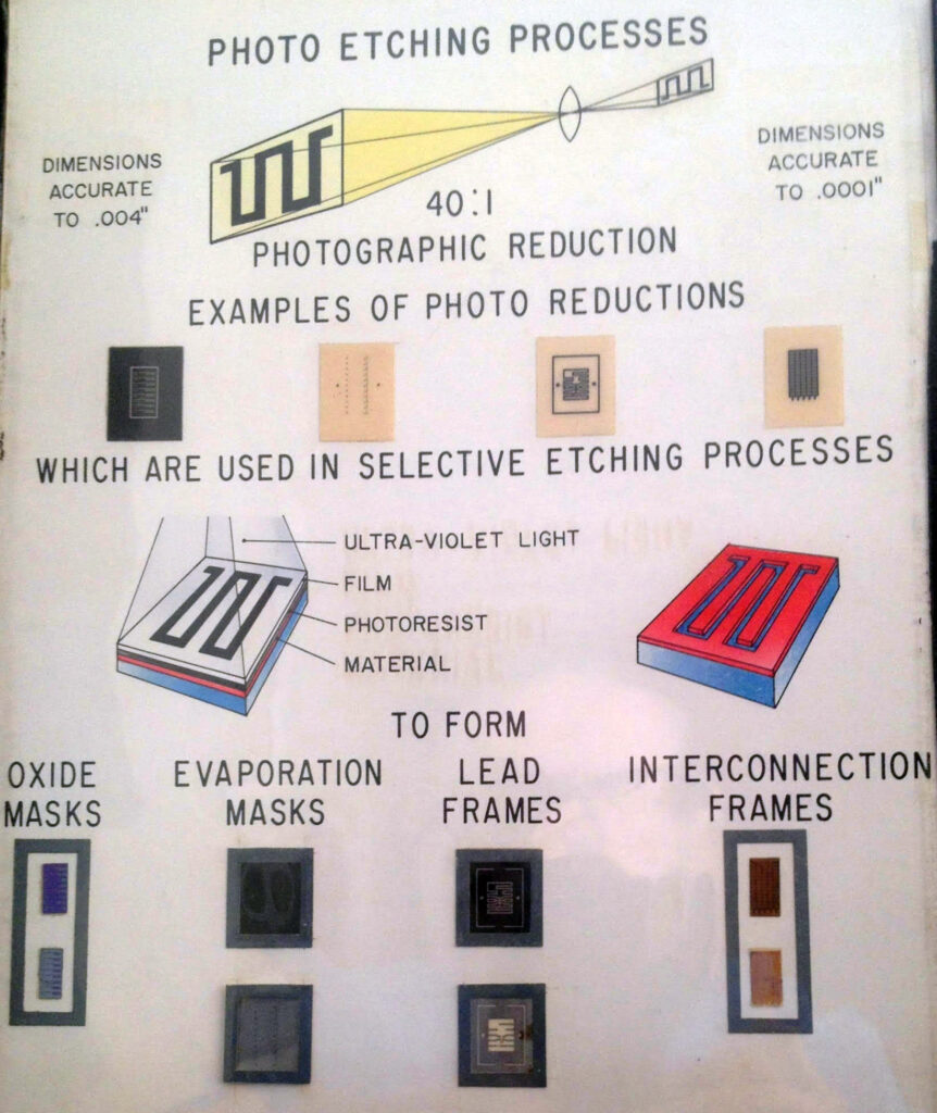
Early TI Photolithography process. Duplicated and enhanced by the Soviet Engineeris.
The main advantage of planar technology, which caused its spread in semiconductor electronics, is the possibility of using it as a method of mass manufacture of semiconductor devices and allows you to reduce the spread of their parameters, keeping specs consistent from one device to another.
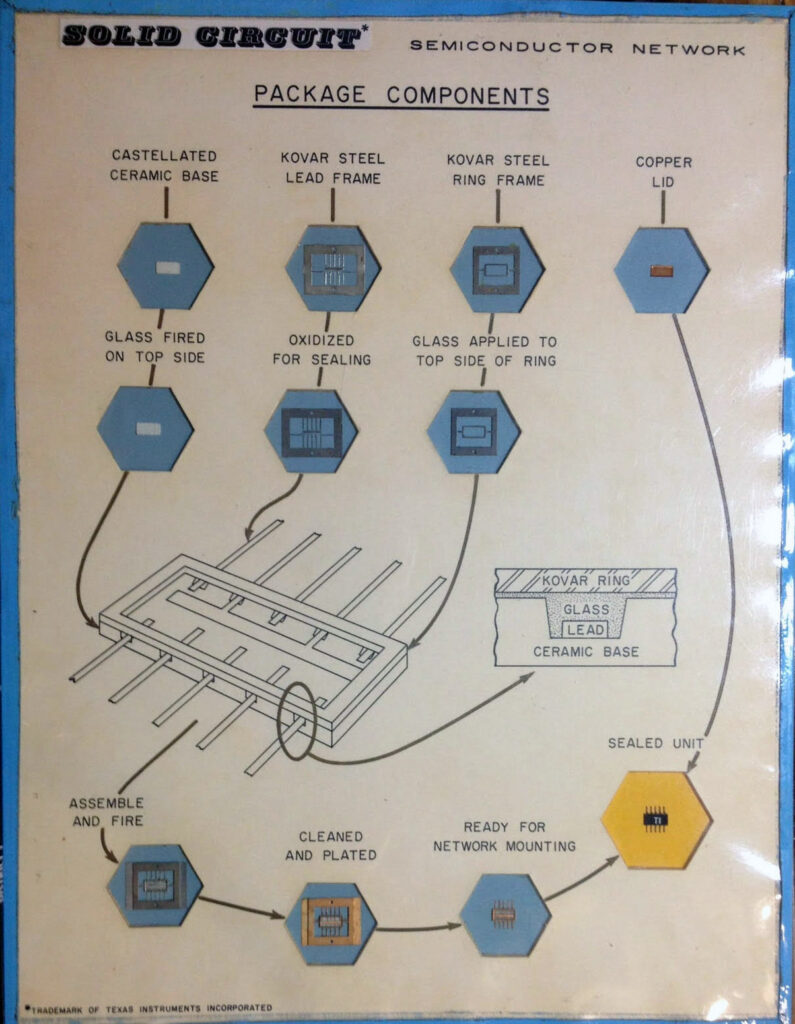
Early TI Assembly Process
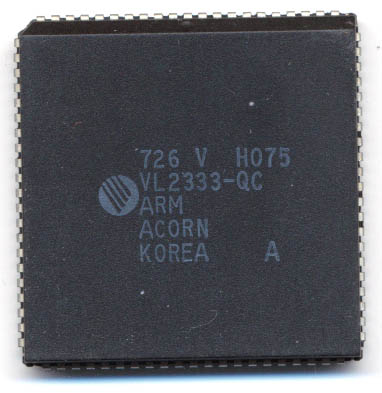
In October 1961, Texas Instruments announced the creation of RCTL (Resistor Capacitor Transistor Logic) SN51X logical planar integrated circuits, and in 1962 began mass production of them. The SN51xz line was an enhanced version of the previous (released earlier that year) SN50x line. The SN51x provided more power (for fanout) and speed, about 10x faster. TI was the first to release six SN510-SN515 chips. Early SN51X series chips sold for over $400 when first released (in 1961 dollars, today, around $4100).
TI SN502
Posted in:
Research