Archive for the 'Just For Fun' Category

December 29th, 2018 ~ by admin

The End is Near (of the year) – A Look Back at Y2K

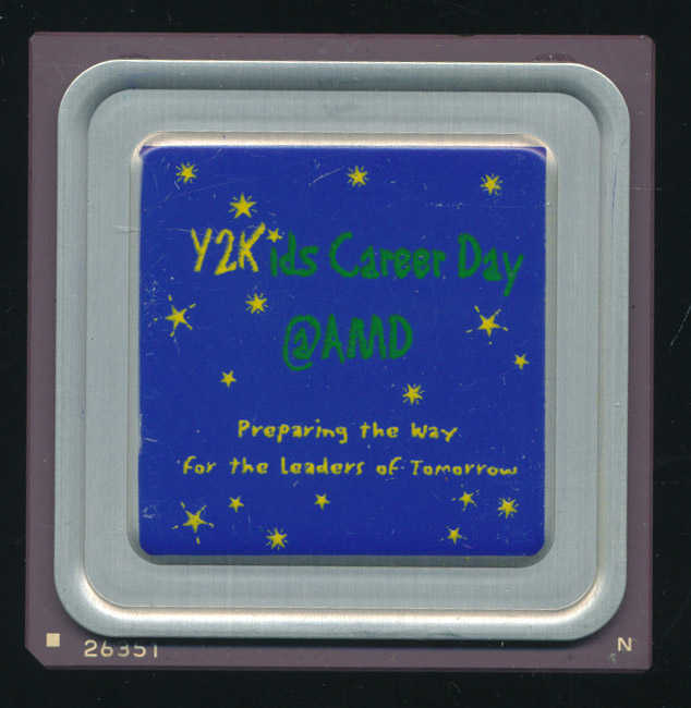
AMD Y2Kids Career Day – K6-2 Custom Painted 

Think back 19 years, the year is 1999 and in just a few days the world is apparently coming to an end due to programmers of the 60’s and 70’s deciding to save precious memory and use 2-digits for the year instead of 4.  Or perhaps they just assumed that in 30-40 years we really wouldn’t be using the same systems. Either way the world (and by world we mean mainly the media) was prepared to go dark as everything technology driven ground to a halt as the clocks struck midnight.  Kids pondered if this would mean an extended holiday break, while parents wondered if they would still have a job, or money in their computer controlled checking account.

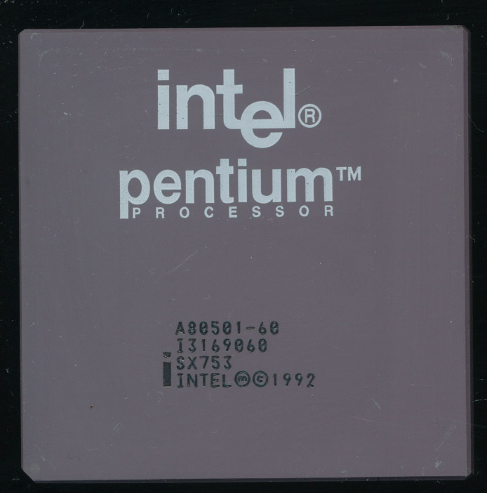
Thankfully (though perhaps looking back that is becoming murky to some) it was a complete non-even, life, and technology continued at a record pace. And who would want to miss it? The GHz war between AMD and Intel was neck and neck at the turn of the millennium, with AMD set to win it by a few days.  This was the age of the Pentium 3, the Athlon and the K6-2.  Technology was glamorous and some of its downsides seen today were relegated to sci fi movies.  AMD and other companies held job fairs to acquire new talent, and also hosted Career Days for younger kids to see what went on in the exciting tech industry.  This specially painted AMD K6-2 CPU was likely handed out during such an event, probably either in Austin, TX (where AMD had a large fab) or Santa Clara, CA.  Its a NTK made package with a AMD package # 26351, the standard from 1998-2000 and used for most all late K6-2 CPUs. The child who likely would have received this, probably a middle schooler at the time would now be around 30, who knows how such an event affected them but it would be neat if they ended up working at AMD (or Globalfoundries) or at the very least sing an AMD powered computer.

May 27th, 2018 ~ by admin

Mainframes and Supercomputers, From the Beginning Till Today.

This article is provided by guest author max1024, hailing from Belarus.  I have provided some minor edits/tweaks in the translation from Belarusian to English.

Mainframes and Supercomputers, From the Beginning Till Today.

Introduction

We all have computers that we like to use, but there are also more productive options in the form of servers with two or even four processor sockets. And then one day I was interested, but what is even faster? And the answer to my question led me to a separate class of computers: super-computers and mainframes. How this class of computer equipment developed, as it was in the past and what it has achieved now, with what figures of performance it operated and whether it is possible to use such machines at home, I will try to explain all this in this article.

FLOPS’s

First you need to determine what the super-computer differs from the mainframe and which is faster. Supercomputers are called the fastest computers. Their main difference from mainframes is that all the computing resources of such a computer are aimed at solving one global problem in the shortest possible time. Mainframes on the contrary solve at once a lot of different tasks. Supercomputers are at the very top of any computer charts and as a result faster than mainframes.

The need for mankind to quickly solve various problems has always existed, but the impetus for the emergence of superfast machines was the arms race of well-known superpower countries and the need for nuclear calculations for the design and modeling of nuclear explosions and weapons. To create an atomic weapon, colossal computational power was required, since neither physicists nor mathematicians were able to calculate and make long-term forecasts using the colossal amounts of data by hand. For such purposes, a computer “brain” was required. Further, the military purposes smoothly passed into biological, chemical, astronomical, meteorological and others. All this made it necessary to invent not just a personal computer, but something more, so the first mainframes and supercomputers appeared.

The beginning of the production of ultrafast machines falls on the mid-1960s. An important criterion for any machine was its performance. And here on each user speaks of the well-known abbreviation “FLOPS”. Most of those who overclock or test processors for stability are likely to use the utility “LinX”, which gives the final result of performance in Gigaflops. “FLOPS” means FLoating-point Operations Per Second, is a non-system specific unit used to measure the performance of any computer and shows how many floating-point arithmetic operations per second the given computing system performs.

“LinX” is a benchmark of “Intel Linpack” with a convenient graphical environment and is designed to simplify performance checks and stability of the system using the Intel Linpack (Math Kernel Library) test. In turn, Linpack is the most popular software product for evaluating the performance of supercomputers and mainframes included in the TOP500 supercomputer ranking, which is made twice a year by specialists in the United States from the Lawrence Berkeley National Laboratory and the University of Tennessee.

When correlating the results in Giga, Mega and Terra-FLOPS, it should be remembered that the performance results of supercomputers always are based on 64-bit processing, while in everyday life the processors or graphics cards producers can indicate performance on 32-bit data, thereby the result may seem to be doubled.

The Beginning

Read More »

March 21st, 2018 ~ by admin

Intel’s Chipped Chips

Early Intel 8080A processor (no date code) chipped and used in a Uni kit

Typically when collecting something, be it coins, cars or CPU’s having the most pristine unblemished example is highly desirable.  However, sometimes, the best example is one that isn’t perfect, in coin collecting it may be a rare double struck coin, or some other flaw that actually makes the coin more valuable.

In the 1970’s Intel put together many development kits for it’s processors.  These were to help engineers, companies, and even students learn how to use Intel’s products. Intel made several kits specifically for University use, including one based around the MCS-80 processor and another around the MCS-48 microcomputer.  The 8080 University kit came with an 8080 processor, and a variety of support chips, including RAM, EPROMs (usually 1702s), clock drivers, bus drivers etc.  They were often a mix of packages, including plastic, and ceramic, with many chips being marked ‘CS‘ which is Intel’s designation for a Customer Sample.

Military MC8080A CS from a Uni kit. Multiple chipped corners. Such damage often was a result of improper packing in an IC shipping tube.

The price of the kits was kept low, the purpose was to get people use to using Intel products, not to make money.  Due to this, Intel tried to build the kits in the most efficient way possible.  Almost every 8080 University kit included a working, but cosmetically damaged C8080A processor.  These were typically the white/gold ceramic variety with a chipped corner.   It was very common to see a MC8080A or MC8080A/B military spec processor in a University kit, the processor would function fine, but had  some damage, enough that it could not be sold as a mil-spec processor (which has requirements for screening out such damage). The damaged chip would simply be tested, stamped ‘CS‘ and stuck in a kit, ths saving Intel money and keeping a working processor from being wasted.   The same thing happened with the MCS-48 University kits, these included chips such as the D8035 or C8748 MCU, and again, often shipped with damaged chips.

It turns out that the most correct, authentic chip, in a University Kit, was the cosmetically challenged, and in a way, this makes them more uncommon and more interesting.  Its due to their damage that they were selected for the special use in a University kit.  The irony is that many times it was the highest end military screened chips, that ended up getting used in one of the lowest end products.

October 14th, 2017 ~ by admin

VLSI: What is this THING?

VLSI VY12338 THING UA-JET238-01 – Made in 1997

VLSI was started back in 1979 by several former Fairchild employees, 2 of which had previously founded Synertek, a connection that becomes important later on.  VLSI is best known for being a contract deign/fab services company.  They excelled at custom, and semi-custom designs for a wide range of customers, as well as acting as a foundry for customers own designs.  They became best known for their part in the development and success of the ARM processor back in the late 1980’s with ACORN.  They manufactured, as well as marketed and sold, several versions of the ARM processor, one of the few processors they actually sold themselves.  They also made a 6502 used by Apple and 65C816 (CMOS 16-bit 6502).  The 6502 was also a processor that Synertek had made back before Dan Floyd, and Gunnar Wetlesen left Synertek to start VLSI.

VLSI went on to fab processors for some of the biggest companies of the 1980’s.  The made the processor for several Honeywell BULL mainframes, built the processor for the HP A990 computer, and made dozens of chips for SGI and WANG.  VLSI also enjoyed wide success in the early 1990’s making chipsets for 486 processors, before Intel began to offer chipsets on their own in the Pentium era.

Unfortunately like LSI, most of VLSI’s designs are relatively unknown to all but them and their customer.  Marking on the chips rarely provide information on who it was made for, and even less on what exactly it does.  The above chip, marked “VY12338 THING UA-JET238-01” seems to be names as an answer to the question “What do we call this thing?”  Certainly seems to be a bit of humor on the part of some engineer.

VLSI was bought by Philips (now NXP) in 1999 so the THING may forever remain an unknown thing.

Tags:
, ,

Posted in:
Just For Fun

September 13th, 2016 ~ by admin

OSIRIS-REx: Bringing Back Some Bennu

OSIRIS-Rex: RAD750 to Bennu

OSIRIS-Rex: RAD750 to Bennu

The Apollo Group  carbonaceous asteroid Bennu is a potential Earth impactor, with a 0.037% likelihood of hitting earth somewhere between 2169 and 2199.  Bennu is thought to be made of materials left over from the very early beginnings of our solar system, making researching them a very tantalizing proposition.  Rather than wait for the small chance of Bennu delivering a sample to Earth in 150 years the thoughtful folks at NASA decided to just go fetch a bit of Bennu.  Thus is the mission of OSIRIS-REx which was launched a few days ago (Sept 8, 2016) aboard an Atlas V 441 as an $850 Million New Frontiers mission.

Somewhat surprisingly there is scant details about the computer systems that are driving this mission to Bennu.  OSIRIS-REx is based on the design of the Mars Reconnaissance Orbiter (MRO), MAVEN and Juno, and thus is based on the now ubiquitous BAE RAD750 PowerPC processor running the redundant A/B side C&DH computers.  This is the main ‘brain’ of the Lockheed Martin built spacecraft.  Of course the dual RAD750s are far from the only processors on the spacecraft, with communications, attitude control, and instrumentation having their own (at this point unfortunately unknown) processors.

REXIS Electronics: Virtex 5QV - Yellow Blocks are Off the Shelf IP, Green Blocks are custom by the REXIS Team. Powered by a Microblaze SoftCore.

REXIS Electronics: Virtex 5QV – Yellow Blocks are Off the Shelf IP, Green Blocks are custom by the REXIS Team. Powered by a Microblaze SoftCore.

One instrument in particular we do know a fair amount about though.  Regolith X-ray Imaging Spectrometer (REXIS) is a student project from Harvard and MIT. REXIS maps the asteroid by using the Sun as an X-ray source to illuminate Bennu, which absorbs these X-rays and fluoresces its own X-rays based on the chemical composition of the asteroid surface. In addition REXIS also includes the SXM, to monitor the Sun’s X-Rays providing context to what REXIS is detecting as it maps Bennu.  REXIS is based on a Xilinx Virtex-5QV Rad-Hard FPGA.  This allows for a mix of off the shelf IP blocks, and custom logic as well. The 5QV is a CMOS 65nm part designed for use in space.  Its process, and logic design are built such as to minimize any Single Event Upsets (SEU), and other radiation induced errors.  It is not simply a higher tested version of a commercial part, but an entirely different device.   Implemented on this FPGA is a 32-bit RISC softcore processor known as Microblaze.  The Microblaze has ECC caches implemented in the BRAM (Block RAM) of the FPGA itself and runs at 100MHz.

It will take OSIRIS-REx 7 years to get to Bennu, sample its surface, and return its sample to Earth.  By the time it gets back, the RAD750 powering it may not be so ubiquitous, NASA is working on determining what best to replace the RAD750 with in future designs.  Currently several possibilities are being evaluated, including a QuadCore PowerPC by BAE, a QuadCore SPARC (Leon4FT), and a multi-core processor based on the Tilera architecture.  As with consumer electronics, multi-core processors can provide similar benefits in space of hogher performance and more flexible power budgeting all with the added benefit (when design for such) of increased fault tolerance.

June 27th, 2015 ~ by admin

The 16-bit Transistor level MegaProcessor

16-bit MegaProcessor ALU

16-bit MegaProcessor ALU

James Newman in Cambridge (UK) is creating a 16-bit discrete Processor Design called the Megaprocessor (there is nothing micro about it).  Not a VLSI version either, a 16-bit processor built of discrete transistors, hand wired, hand soldered, with debugging provided by…3500 LEDs.  He admits perhaps things got a bit out of hand when a co-worker remarked that it would be helpful if a signal had an LED on it, thus providing the motivation to go out and build a complete 16-bit processor.

James estimates that the design (he is still building it) will take 14,000 discrete transistors, 3,500 of which are actually to drive the LEDs.  ROM and RAM (256 bytes each, assuming he doesn’t get carpal tunnel from soldering it all) will be an extra 16,000+.

An original Intel 8086 used 29,000 transistors, and was a similar 8/16 bit architecture.  The Novix NC4016 stack processor, also 16-bits, was a very clean design using only 16,000 transistors.  HPs original BPC 16-bit processor from 1975 was 6,000, so James design is certainly inline with expectations (though his sanity maybe in question).

While this seems like a crazy amount of work (it is), This is how the first transistor computers were made.  The original DEC PDP-1 from 1959, used 2,700 discrete transistors, and was an 18-bit design.  The Apollo Guidance computer from 1966 was a 16-bit design (using IC’s with 3 transistors each, so a bit easier construction) used 12,300.

So while James’ design may be a bit over the top, it provides a good look back at where we have come.  Today chips can have well over a billion transistors on a die smaller then a fingernail.

Posted in:
Just For Fun

March 29th, 2015 ~ by admin

I Just Poured Water on my Scanner….

Chip that come into the museum are all scanned on a Canon 5600F flatbed scanner.  It has a good (there is some better though) depth of field, and its fast.  Typically chips are scanned at 300dpi, or for small ones (or ones that have a die visible) 600dpi.  This keep the file sizes reasonable, yet still allows them to be studied in good detail on CPUShack.com as well our records.

There are on occasion chips that are VERY hard to scan, either the markings are very small, or very shallow.  This is becoming common on more modern chips, for one the chips themselves are smaller, and second, they are most often laser marked, and there isn’t enough thickness in the package (or die on some) for the Grand Canyon engraving of the 80’s.

1200 dpi dry scan

1200 dpi dry scan


This is a Intel QG80331M500 IO Processor made by Intel in 2007.  It is the replacement for the 80960 based I/O processors, using instead a 500 MHz XScale ARM Processor core.  This scan was done at 1200 dpi, the part number is visible, barely, but the S-spec and FPO (lot code) are not.  The markings are laser etched directly onto the surface of the silicon die.  This is fairly common on this type of chip (as well as most all of Intel chipsets).  How do we improve upon this?  Bumping the resolution to 2400dpi just makes a bigger blurry picture (with more noise).  What we need is better resolution, at where the scanner works best (less noise at 1200 dpi scan).

Thankfully we can use a ‘technology’ that is very much similar to how modern processors themselves are now made.  Dumping water on the scanner, also known as immersion scanning.

Read More »

December 20th, 2014 ~ by admin

Monsanto: Bringers of the Light

Monsanto MCT2 - LED Based Opto-coupler

Monsanto MCT2 – LED Based Opto-coupler

This little chip, dated from 1973, is part of the history of what we are surrounded by, LEDs.  And they have an unlikely and somewhat surprising beginning.  The MCT2 is an opto-coupler, basically an LED and a phototransistor in a single package, used for isolating digital signals.  The important portion here is the LED.  LEDs are in nearly every electronic product these days, and this Christmas season we see many Christmas lights that are now LED based.  THey are more efficient, and much longer lasting.  Certainly the eco-friendly choice for lighting.  And they have their roots in a company that does not always elicit an eco-friendly discussion.

That would be Monsanto.

That big ‘M’ on the package is for Monsanto, who from 1968-1979 was the leading supplier of LEDs and opto-electronics.  In 1968 there were exactly 2 companies who made visible light LEDs (red), HP and Monsanto, and HP used materials supplied by Monsanto to make theirs.

LED Christmas Lights

Read More »

October 15th, 2014 ~ by admin

Has the FDIV bug met its match? Enter the Intel FSIN bug

Intel A80501-60 SX753 - Early 1993 containing the FDIV bug

Intel A80501-60 SX753 – Early 1993 containing the FDIV bug

In 1994 Intel had a bit of an issue.  The newly released Pentium processor, replacement for the now 5 year old i486 had a bit of a problem, it couldn’t properly compute floating point division in some cases.  The FDIV instructions on the Pentium used a lookup table (Programmable Logic Array) to speed calculation.  This PLA had 1066 entries, which were mostly correct except 5 out of the 1066 did not get written to the PLA due to a programming error, so any calculation that hit one of those 5 cells, would result in an erroneous result.  A fairly significant error but not at all uncommon, bugs in processors are fairly common.  They are found, documented as errata, and if serious enough, and practical, fixed in the next silicon revision.

What made the FDIV infamous was, in the terms of the 21st century, it went viral.  The media, who really had little understanding of such things, caught wind and reported it as if it was the end of computing.  Intel was forced to enact a lifetime replacement program for effected chips.  Now the FDIV bug is the stuff of computer history, a lesson in bad PR more then bad silicon.

Current Intel processors also suffer from bad math, though in this case its the FSIN (and FCOS) instructions.  these instructions calculate the sine of float point numbers.  The big problem here is Intel’s documentation says the instruction is nearly perfect over a VERY wide range of inputs.  It turns out, according to extensive research by Bruce Dawson, of Google, to be very inaccurate, and not just for a limited set of inputs.

Interestingly the root of the cause is another look-up table, in this case the hard coded value of pi, which Intel, for whatever reason, limited to just 66-bits. a value much too inaccurate for an 80-bit FPU.

August 13th, 2014 ~ by admin

What’s Missing?

Four-Phase Systems: 1969-1981

Four-Phase Systems: 1969-1981 (click to enlarge

What’s Missing from this Four-Phase Systems family portrait?  Hopefully the lost member arrives this week.  Anyone remember Four-Phase?

Posted in:
Just For Fun