Archive for January, 2013

January 26th, 2013 ~ by admin

CPU of the Day: New Logo – Old Processor: Intel 486 DX2 66

Intel 486 With new logo - 2007

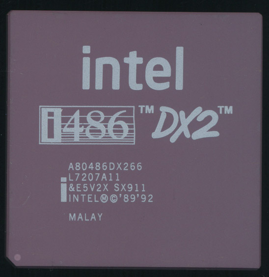
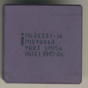
Intel 486 With new logo – 2007

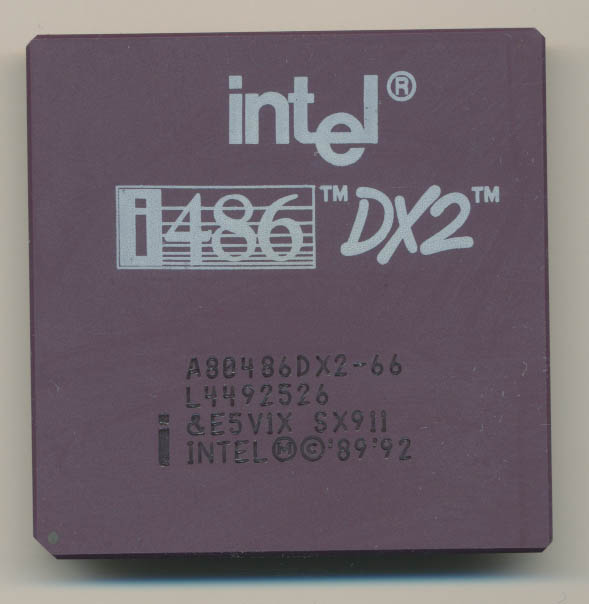
Intel introduced the 486 in 1989, 24 years ago so it may be a bit surprising to see a 486 with the more modern Intel non-‘dropped e’ logo.  Intel began using the current logo in 2006, well after the height of the 486 market.  However Intel continued to make several 486 processors clear up through 2007.  These went to supply many embedded applications (medical, industrial, etc) that had originally been designed with a 486 and remained in production.  These types of devices either did not need a better processor or due to regulatory reasons, could not use one.  This is actually a common issue with medical devices, once designed, they are certified by the FDA (in the US, other agencies in the EU, Canada etc).  This certification is very specific to that exact hardware.  Often you cannot even change the S-spec/revision of the processor.  If it was built/certified with an SX911 A80486DX2-66 that’s what it must continue to use.  Re-certification is very expensive and time consuming.  It may seem overkill but these type of applications are often life sustaining, a failure could mean more then a reboot and lost game of Doom.  This is why Intel (and other companies) will choose a few products out of each line to be long-term production, this helps engineers select a product to design into their device, that has a guaranteed production life.  Currently Intel’s long term products guarantee a 7-year production.

Original DX2 Late 2004

Original DX2 Late 1994

This particular chip was made in April 2007. Intel announced it would be discontinued by the end of 2007 so this is truly one of the last (Intel) 486s ever made.  It is a SX911 &E5V2X version which is an SL Enhance (&E) 5 Volt Mobile (2X) processor.  The 2X means that the processor requires 2 external clocks, typically one would be used for when a laptop was plugged in (full speed, 33MHz in this case) and a second, which could be anything lower, for battery operation.  Obviously these can be implemented in any application, not just a laptop.  Registers contents, interrupts  etc are all preserved when the processor switches clock frequency so this is done on the fly, just like today’s processors.  The SX911 spec, which first was released in 1994, came in both 1X (desktop) and 2X (mobile) versions.  Throughout its 13 years of production it remained on a 150mm (6-inch) wafer process at 0.8u.

Posted in:
CPU of the Day

January 18th, 2013 ~ by admin

CPU of the Day: Cypress CY7C601 25MHz SPARC

Cypress CY7C601-25GC

Cypress CY7C601-25GC – First package with heatspreader – Omitted on later versions

In Mid-1987 Sun Microsystems (now owned by Oracle) released the SPARC (Scalable Processor ARChitecture)  processor architecture to be used in their computers (replacing the 68k based systems they had previously used).  The SPARC was designed from the outset to be an open architecture, allowing manufactures to license and built processors that implemented it using whatever technology they wished.  The goal of this was to 1) build a large SPARC ecosystem and 2) keep prices in check by fostering competition among manufacturers.  The SPARC is still used today by Oracle, Fujitsu, the European Space Agency and others, owing largely to its design as an open architecture from the very beginning.

The first version was made by Fujitsu on a 20,000 gate array at 1.2 micron and ran at 16.6MHz.  In July 1988 Cypress  (later to be spun off as Ross and make the famous HyperSPARC line) announced the CY7C601.  This was the fastest implementation of the SPARC at the time.  It was made on 0.8u CMOS process and contained 165,000 transistors, dissipating around 3.3Watts.  As was typical of many processor designs of the time, it was an integer only processor, requiring a separate chip (the CY7C602) for floating point work.  In September of 1988, Cypress cross licensed the ‘601 to Texas Intruments in exchange for rights to the 8847 floating point processor.  This was mainly to appease one of Cypress main customers who demanded that a second source for the ‘601 chips be available, a demand more common in the 1970s then in 1988 but Cypress obliged.  Cyrpress also gained the rights to make the next generation SPARC processor that TI was developing.  TI would go on to make many SPARC processors, and continued to be the primary fab for Sun up through the SPARC T2 Plus in 2008.  Oracle now used TSMC to fab the T3 and T4 SPARC processors.

Tags:
, , ,

Posted in:
CPU of the Day

January 12th, 2013 ~ by admin

The Intel 80186 Gets Turbocharged – VAutomation Turbo186

Original Intel 6MHz 80186 Made in 1984

Original Intel 6MHz 80186 Made in 1984

2012 marked the 30th anniversary of the introduction of the Intel 80186 and 80188 microprocessors.  These were the first, and arguably only, x86 processors designed from the beginning as embedded processors.  It included many on-chip peripherals such as a DMA channels, timers and other features previously handled by external chips.  Initially released at 6MHz, clock for clock many instructions were faster then the 8086 it was based on, due to hardware improvements.

In 1987 Intel move the 186 to a CMOS process and added more enhancement including math co-processor support, power down modes and a DRAM refresh controller.  Speeds were increased up to 25MHz (from the 10MHz max of the NMOS version).  Through the years Intel continued to developed new versions of the 186 with added features, lower voltages, and different packages.  It was not until 2007 that Intel finally stopped production of the 186 series.  It continued to be made by others under license including AMD, who made versions running up to 50MHz.  Fujitsu and Siemens also produced the 186 series. Like the 8051 the 186 gained significant support, being embedded in millions of devices.  The instruction set was familiar, debugging and development systems were (and are) plentiful so the 186 core continues to be in wide use.

As IC complexity and transistor counts increased the need for a processor core that could not just be embedded into a system, but be embedded into a custom ASIC or SoC became apparent. IC’s were being designed to handle things like DVD playback, set-top boxes, flat panel control and more.  These applications still required some sort of processor to handle them but having to have a separate IC for it was not economical.

pixelworks PW166B - 67MHz Tubro186 based Flatpanel Controller made in 2004

pixelworks PW166B – 67MHz Tubro186 based Flatpanel Controller made in 2004

VAutomation (founded in 1994) designed Verilog and VHDL synthesizable cores (meaning they could be ‘dropped’ into an IC design or FPGA).  In November 1996 VAutomation licensed the 8086/8, 80186/8 and the CMOS versions from Intel.   This gave them them ability to design their own compatible models of these processors without fear of litigation.  More importantly it allowed them to sub-license these designs to others.  In 1997 VAutomation demo’d their first 186, the V186 core.  This was a Intel 80186 compatible core that could be synthesized into a customers design.  It was ‘technology independent  which means it was not restricted to a certain process or even technology.  It could be used in CMOS, ECL, 0.35u, 1 micron, whatever the client needed.  On a 0.35u CMOS process it was capable of speeds in excess of 60MHz, and did so with less then 28,000 gates. One of the first licensees was Pixelworks, which made controllers for monitors.  Typical licensing was a $25,000 fee up front and royalties on a per device basis usually split into a high volume (over 500,000 units) and low volume.  Typical price per chip was $0.25-$2.00, which was cheaper then the $15 price Intel was charging for a discrete 80C186.

Read More »

January 8th, 2013 ~ by admin

Repair or Replace? Not always a choice.

A very interesting post by Jack Ganssle over at Embedded.com about his adventures and lessons learned from a trip to the Bahamas and a chat with the engineer charged with maintaining an island Intel 8085 based telecom system.  An apt discussion especially with the CES (Consumer Electronics Show) going on, an event showcasing the latest and greatest of what mostly is ‘disposable’ technology.

Many devices, however, must still be built for areas, industries, and regions where replacement is simply not a viable option, whether its because of remoteness or lack of parts.  In the early days of computing surface mount devices were few and far between.  The DIP rained supreme, and the end user was often very good at debugging with simple tools.  Sockets made repairing boards much easier and even discrete resistors could be changed out without much trouble.  Upgrading your computer often involved replacing the processor with a faster one, then changing the clock crystal to support it, and switching out individual RAM chips to ones with a faster access time to support the now faster processor.  You then used the left over parts to either repair another system, or build another project.

From the article:

“Here in Staniel Cay there’s no FedEx; no UPS; no postal system. The mail boat arrives once every two weeks, more or less, if the weather is good. Occasionally it sinks.”

JITS (Just In Time Supply) is simply not an option there. And its not just the Bahamas where repair is the only option. It’s not limited to non hi tech areas.  When something breaks in space, perhaps the most hi tech environment of all, you can’t go to town and get new parts, you have to make do, that’s real engineering.  Apollo 13 showed how things could be repaired with very unusual articles, and similar ‘fixes’ are common on the International Space Station.

Give it a read, its as entertaining as it is educational.

Posted in:
Just For Fun

January 7th, 2013 ~ by admin

2012: Year in Review: UV EPROMs

Unusual double marked Intel HC2708. Intel used 'H' for a brief time to denote a windowed DIP package.

Unusual double marked Intel HC2708. Intel used ‘H’ for a brief time to denote a windowed DIP package.

UV-EPROMs are a technology made obsolete in an incredibly short period of time by widely available, and more flexible, Flash and EEPROM technology.  Processors evolved, DRAM and SRAM evolved, EPROMs simple ceased to exist.  There were attempts to make them faster, lower-power, or in more convenient packages, but at the end of the day (or the end of the 90’s) shining a UV light into a small round window to erase them simply became a sign of an era long passed.  That window, however, also allows for the beauty and in some cases massiveness, of their silicon dies to be seen by all, something today’s black plastic flash simply cannot do.

Here are a few of the interesting EPROMs I found in 2012 (click to enlarge)


AMIS5204A-7604

AMI made many custom chips for clients, as well as second sourced various designs.  This is a S5204A, a copy of the National Semiconductor MM5204.  Made in 1976 it stored 4kbits and had a ‘fast’ access time of only 750ns.  It could be fully programmed in ‘less then a minute’ and took ‘only’ 10 minutes to erase all 4096 bits.  Power draw was 750mW max, about the same as a 800MHz Intel Atom processor.

AtmelAT27C256R-55LC_600dpi

The Atmel AT27C256R-55LC was a CMOS 55ns 256kbit EPROM in a surface mount package.  Made in late 1996 it was the beginning of the end for EPROMs.

IntelC27C202-70V05-ES

Intel used some unusual packages for a few of their EPROMs.  This package was more commonly used on things like C8751s.  Here it is a C27C202-70V05 Engineering Sample.  This is a 2Mbit EPROM.

SovietK573RF5-8903

No EPROM collection is complete without at least a few examples of Soviet EPROMs.  If anything for their amazing packages.  Here a Soviet of unknown plant K573RF5 made in 1989.  This is a clone of the Intel 2716.

TITMX2532-35NL

The Soviet bloc mastered making EPROMs with plastic packages, but this never caught on in the western market.  I have never seen a production EPROM in a plastic package out side of East German/USSR.  However I did acquire a plastic TI TMX2532-35NL.  TMX denotes it as a prototype.

WSI27C256L-15-5962-8606305XA

The military and industrial markets continued to use EPROMs far longer then the commercial/consumer markets.  Cost being less of a concern then reliability.  EPROM’s had a proven track record and thus were used until Flash had proven itself.  This is a Waferscale Integration (WSi) 27C256L-15 mil spec EPROM.

Tags:
, ,

Posted in:
EPROM of the Day

January 5th, 2013 ~ by admin

2012: Year in Review: Processors and FPUs

Welcome to 2013!  2012, was a busy year here at the CPU Shack Museum. We added 716 new processors/EPROMs/MCUs, which works out to an average of 2 new chips per day.  This includes 16 New in Box Processors. We also added 53 new Graphics Processors, which isn’t bad for something we only collect on the side.

Some processor highlights (in no particular order, click to enlarge):

HPIB21364-1300VP7

Here is a HP/Compaq 21364 1300MHz, this was the end of the road for the DEC Alpha architecture.  It was killed off in favor of the Itanium, for better or for worse.

IBMPOWER5+19GHz

The IBM POWER5+ MCM is a stunning chip to look at, clocked at 1.9GHz its a dual core with on package L3 cache

IntelMG80387-16-SM156

An Intel MG80387-16 SM156 US Military MIL-STD-883B spec math co processor for the 80386 processor.  Made in 1990

MME80A-CPU-9107

Going back in time further is this East German (MME) 80A CPU, a clone of  the Zilog Z80 made in 1991 (copied before unification, produced after, for this example).  Its always neat to see the white ceramic package, even well into the 1990’s.

NexGenNx586-P133-D-J

NexGen was a company that became victim of the wild processor wars of the 1990’s.  It was bought out by AMD which used its designs as the basis of the very popular and successful AMD K6.  Here is a very uncommon 133 (rated) without FPU.  Later they made a version with an integrated FPU.

ZoranZR36762PQC-Turbo186

And to get all the way to ‘Z’ we shall go to the Zoran ZR36762.  Its a DVD controller SoC, with Dolby Digital support.  Not something one sees and thinks of as a processor.  However at its core, even in 2004, it is not an ARM, its not a MIPs, its a high speed (67MHz) Turbo186, the same 186 architecture Intel released in 1982, still being used, albeit in CMOS.

In the next few days I’ll post some EPROM highlights, then some GPU highlights.  2013 is already off to a great start with new chips coming in each week.

Tags:
, , , , ,

Posted in:
CPU of the Day