Archive for September, 2012

September 27th, 2012 ~ by admin

EPROM of the Day: AMD AM27C2048 – Shrinking Dies

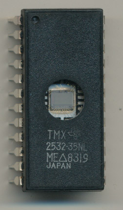
AMD AM27C2048-150DC – 3 Dies (Click to view larger)

In the semiconductor industry process shrinks are highly sought after.  They result in smaller die sizes for the same part, which results in more chips per wafer, thus increasing revenue.  There are other benefits (typically speed increases and power decreases (aside from leakage)) but from a purely economical stand point, the smaller dies result in more profits.

Rarely do you get to SEE the result of these process changes.  UV-EPROMs fortunately have a window, for erasing them with UV light, that also lets the die be seen.  Here are three AMD AM27C2048 EPROMs.  These are CMOS 2-Mbit EPROM, pretty common in the 1990s.  As you can see that while they are all the same part, the dies are significantly different. While its hard to say for sure without a die analysis, we can make some good estimations based on what foundries AMD had at the time these devices were made.  The first EPROM is date late 1993 which will likely be a 1 micron process.  The second EPROM, dated mid 1997 is a bit smaller, around 20% smaller, which fits with AMD’s 0.8 micron fabs.  The last, and latest, EPROM was made in 1998, likely at the joint AMD-Fujitsu (FASL) plant in Japan.  This would mean it is a 0.5 micron device. The plant was transitioning to 0.35 micron at the time, but that was most likely used for the higher profit Flash memory devices.  By 1998 EPROM’s were on the decline.

Also of note is the different copyrights.  The first two are copyright 1989 while the third is 1997.  Its hard to know for sure (I do not have the microscopes/tools needed to do die analysis) but it is likely the 1 micron to 0.8 micron was an optical shrink. Literally this means that the die (and masks) are scaled down to a new smaller process with no architectural changes.  This is simple and inexpensive.  Sometimes changes will have to be made to support a new process, or make full use of its benefits, so a new layout/masks are made.  This is likely the case with the 1997 copyrighted EPROM.  The design was altered to work with the new, smaller process, and it was significant enough to warrant a new copyright.

Tags:
,

Posted in:
EPROM of the Day

September 21st, 2012 ~ by admin

CPU of the Day: MicroModule Systems Pentium Gemini

MicroModule Systems GV1-D0-3S-60-120A 120MHz (top side)

MicroModule Systems (MMS) began operations in 1992, following the completion of an agreement to acquire the assets and license rights to the technology of Digital Equipment Corporation’s MCM (Multi-chip Module) engineering and manufacturing business in Cupertino, California. The MicroModule Systems vision was to lead the next wave of electronic integration technology. Previous waves have been: discrete components (1950s), integrated circuits (1960s), large-scale integration (1980s), and system on a chip (mid 1990s).

The MMS Gemini was a module, that includes the National Semiconductor chipset die (x2) , a P54CSLM Pentium die, tag RAM, and cache RAM (128Kx2) as well as an LM75A temperature sensor for thermal management.   MMS used Intel D0 revision P54 processors (with the exception of some early C0 die), a stepping Intel never packaged themselves (it was solely used for the ‘known good die’ program).  When Intel discontinued selling fully tested dies, MMS had no way to build the Gemini and later MMX modules, so in 1998 went out of business. The Gemini was used in many mobile, and rugged PC applications such as the Motorola MW520 Computer used in many police cars.

MMS also produced MCM modules for ROSS, used to make the HyperSPARC processor as well as the Intel Pentium Pro 1MB MCM.   For a company that was only in existence for 6 years, their impact was tremendous. MMS was not alone in their production of Intel Pentium Processor modules…

Fujitsu also made modules using Intel dies.  These were again used in rugged PC applications, laptops, and industrial computers.

Fujitsu MRN-3546 120MHz

Fujitsu made 100, 120, 133, and MMX processors on a MCM type package where the individual components are bonded/soldered to a ceramic substrate (rather then the PC Board)

Tags:
,

Posted in:
CPU of the Day

September 16th, 2012 ~ by admin

EPROM of the Day: Plastic MME U552D – Intel 1702 Clone

MME U552D – Plastic 1702

Today’s EPROM is a very rare early prototype from MME (VEB MikroElektronik “Karl Marx” Erfurt ).  Part of the East German state-owned electronics business.  MME (and their predecessor FWE) made clones of Intel 1702, 2708-2764 EPROMs as well as many processors.  These were all unlicensed, reverse engineered, or copied via industrial espionage since this was all before the end of the USSR, and the technology blockade put in place to ‘prevent’ Eastern Europe from using Western technologies.  This particular U552D is a clone of an Intel 1702A, however, it is made in a plastic package (with what appears to be a actual quartz window).   A very unusual package that was used in Soviet devices mainly and very rarely in the west.

The only western EPROM I have found in plastic is a prototype TMX2532-35NL from Texas Instruments (thus the TMX prefix).


However, the MME U552D actually has the window glued to the top of the plastic package, rather then integrated into it like the TI, and the Soviet designs.

Tags:
,

Posted in:
EPROM of the Day

September 6th, 2012 ~ by admin

Apple iPhone Update: Whats changed since the iPhone 4

Back in 2010 we did a write up on the many processors in each iPhone for each version through the iPhone 4.  Since then Apple has released the iPhone 4 (CDMA) and the mid-cycle refresh iPhone 4S.  Seeing as the iPhone 5 should be released on September 12th here is a quick update to bring our table up to date.

CPUs by function and generation of iPhone:

Function 2G 3G 3GS 4 4-CDMA 4S
App Processor Samsung S3C6400 400-412MHz ARM1176JZ Samsung S3C6400 400-412MHz ARM1176JZ Samsung S5PC100 600MHZ ARM Cortex A8 Apple A4 800MHz ARM Cortex A8 Apple A4 800MHz ARM Cortex A8 Apple A5 900Mhz Dual core ARM Cortex-A9
Baseband S-GOLD2 ARM926EJ-S <200MHz Infineon X-Gold 608 ARM926 312MHz + ARM7TDMI-S Infineon X-Gold 608 ARM926 312MHz + ARM7TDMI-S X-Gold 618 ARM1176 416MHz Qualcomm MDM6600 ARM1136JS 512MHz Qualcomm MDM6610 ARM1136JS 512MHz
GPS NA Infineon HammerHead II Infineon  HammerHead II BCM4750 (no CPU core) see above see above
Bluetooth BlueCore XA-RISC BlueCore XA-RISC BCM4325 (2 CPU cores) BCM4329 (2 CPU cores) BCM4329 (2 CPU Cores) BCM4330ARM Cortex-M3 + Bluetooth CPU
Wifi Marvell 88W8686 Feroceon ARMv5 128MHz Marvell 88W8686 Feroceon ARMv5 128MHz see above see above see above see above
TouchScreen Multi-chip BCM5974 TI TI TI TI
OS Nucleus by Mentor Graphics Nucleus Nucleus ThreadX by ExpressLogic REX by Qualcomm REX by Qualcomm
Total Cores 5 7 7 5 5 6

Apple iPhone 4 CDMA

The CDMA version of the iPhone 4 switched from an Infineon X-Gold baseband to a Qualcomm MDM6600 running a 512MHz ARM1136JS core.  Interestingly this baseband supports GSM but due to antenna issues it is not implemented here. The Qualcomm Gobi, as it is known, also has integrated GPS, removing the need for the old Broadcom BCM4750.  This sets the stage for the iPhone 4S.

Read More »

Tags:
, ,

Posted in:
Processor News

September 6th, 2012 ~ by admin

Intel vs. The World – The Infamous ‘338 Patent

A Brief History

Long before the mess of Apple vs. Samsung (and seemingly everyone else), there was another famous company, with a patent in hand, that it seemed everyone was violating.  The issue of Intellectual Property (IP), and its associated patents has long been an issue in the technology business, and certainly in the business of CPU’s.  There are many many functions inside a CPU, different structures for handling instructions, memory access, cache algorithms, branch prediction etc.  All of these are unique, intellectual property.  It doesn’t matter if you implement them with a slightly different transistor structure, as long as the end product is relatively the same, there is the risk of violating a patent.  Patents are tricky things, and litigating them can be very risky.  You must balance the desire to keep competition from violating your IP, but at the same time minimize the risk that your patent is declared invalid.  This is why most cases end up in an out of court settlement, usually via arbitration.  Actual patent jury trials are fairly rare, as they are very expensive and very risky to all parties involved

Infringing?

In the early days (1970’s and early 1980’s) there was routine and widespread cross licensing in the industry.  Many companies didn’t have the fab capacity to reliably meet demand (IBM wouldn’t purchase a device unless it was made by at least 2 companies for this very reason) so they would contract with other manufacturers to make their design.  Having other companies manufacture your design, or compatible parts, also increased the market share of your architecture (8086, 68k etc).  For years AMD made and licensed most everything Intel made, AMD also licensed various peripheral chips to Intel (notably the 9511/2 FPU).  As the market grew larger, the competition increased, Intel (and others) began to have enough reliable fab capacity to safely single source devices.  Meanwhile other companies continued to make compatible products, based on previous licensing.  AMD notably made x86 CPU’s that ate into Intel’s market share. In the 1970’s Intel had cross license agreements with AMD, IBM, National, Texas Instruments, Mostek, Siemens, NEC and many others.

Read More »

Posted in:
Research