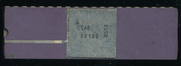
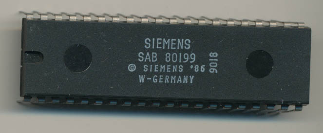
RCA CDP1855: A Multiplier for the COSMAC
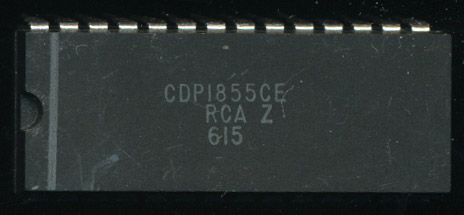
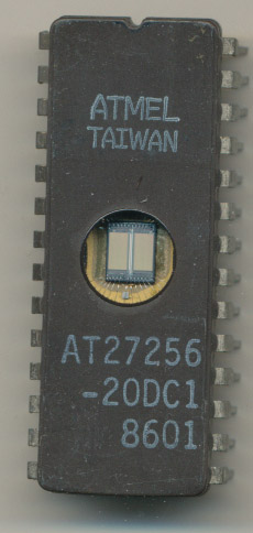
RCA CDP1855CE – 3.2MHz @ 5V
In the 1970’s MULT/DIV instructions were fairly uncommon to be implemented in hardware on a processor. They were implemented in software (usually be the compiler, or hand coded) as a series of adds and subtracts/shifts. In some cases dedicated hardware, usually through a series of bit slice processors, or ‘181s were added to handle MULT/DIV requirements.
In 1978 RCA announced the CDP1855 Programmable Multiplier/Divider for the 1802 COSMAC processor. Sampling began in 1979, making this one of the earliest ‘math coprocessors’ of the time. The 1855 was an 8×8 Multiplier/Divider, handling Multiplies with Addition/Shift Right Ops, and Division using Subtractions/Shift Left Ops. It was, like the COSMAC, made in CMOS, and at 10V ran at 6.4MHz, allowing for a 8×8 MULT to finish in 2.8us. The CDP1855 was also designed to be cascaded with up to 3 others, providing up to a 32×32 bit multiply, in around 12usec, astonishing speed at the time. Even the slower CDP1855CE (using a 5V supply and clocked at 3.2usec) could accomplish a full 32×32 MULT in 24usec. An AMD AM9511 (released a year earlier) can do a 32×32 fixed point multiply in 63usec (@ 3MHz).
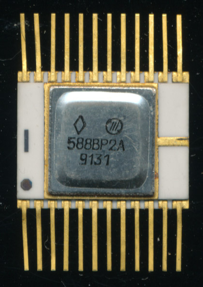
Soviet Integral 588VR2A – CDP1855 ‘Analog’ from 1991
The CDP1855 was designed to interface directly with the 1802 processor, but could be used with any other 8-bit processor as well. It was programmable, so the host processor only needed to load with the data to be multiplied/divided, the control values ot tell it what to do, and then wait for the results.
As was typical, the Soviets made an ‘analog’ of the CDP1855 called the 588VR2 and 588VR2A. The 588VR2 was packaged in a 24-pin package vs the 28 pins of the CDP1855, so its certainly not directly compatible. Soviet IC design houses were instructed and paid to design and make copies of Western devices, typically original ideas were discouraged. This led to a lot of devices being made that were similar, but not the same as their Western counterparts, the design firm could make a somewhat original device, and then simply claim to the bureaucrats that it is an ‘analog’ to a certain Western design. Thus the 588VR2 is ‘similar’ or an ‘analog’ to the 1855.
The CDP1855 continued to be made, and sold into the late 1990s, much like the 1802 processor it supported.