First Start of IC Collecting
This will be the beginning of a three part series on Vintage IC Collecting, as I get asked a lot, ‘why do you collect computer stuff?’ and How do you do it? Where do you find chips etc.
Part 1: Why Collect Vintage Chips?
Part 2: What Vintage Chips should I Collect?
Part 3: How do I collect Vintage IC’s?
These really are the fundamentals to collecting/curating anything, and are important if you wish to have any structure to your hobby of collecting. Collecting itself seems to be built into human nature, and psychologists and evolutionary scientists have many theories as to why.. Freud, who else, claimed that people collect things due to ‘unresolved toilet training issues.’ Others see collecting as a evolutionary strength, that allowed for a better chance of survival, those that collected scarce resources, had a better chance of living to procreate.
Myself, I started collecting coins when I was young, among other things. While scrapping out computers in High School I figured the processors should be saved, as the ‘brains’ of the computer, and thus my hobby, and the museum, began.
The Collection Progresses
There really has become two main reasons for continuing to do so. First, I see a need to preserve some small portion of the technology that has driven us to where we are today, and where we are going. Second, its genuinely fun, the hunt for new chips, the research into finding where they were used, and why they were made and the camaraderie with fellow collectors.
This leads us to the Why, specifically for collecting Vintage IC’s. Many assume that those who collect computer chips will be ‘a bunch of nerds’ and while some certainly are, there is a great variety. Like other collecting areas, there are those who collect for economic reasons, they see a good deal, buy it, with the intent of reselling it for profit at some later date, and there is certainly nothing wrong with this. Others have some historical connection with the chips they collect. They may be retired Electrical/Computer Engineers, programmers and the like, that see collecting as a way to preserve some of what they did.
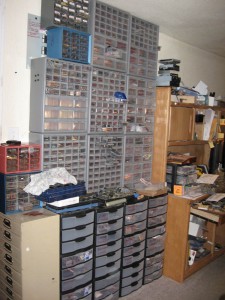
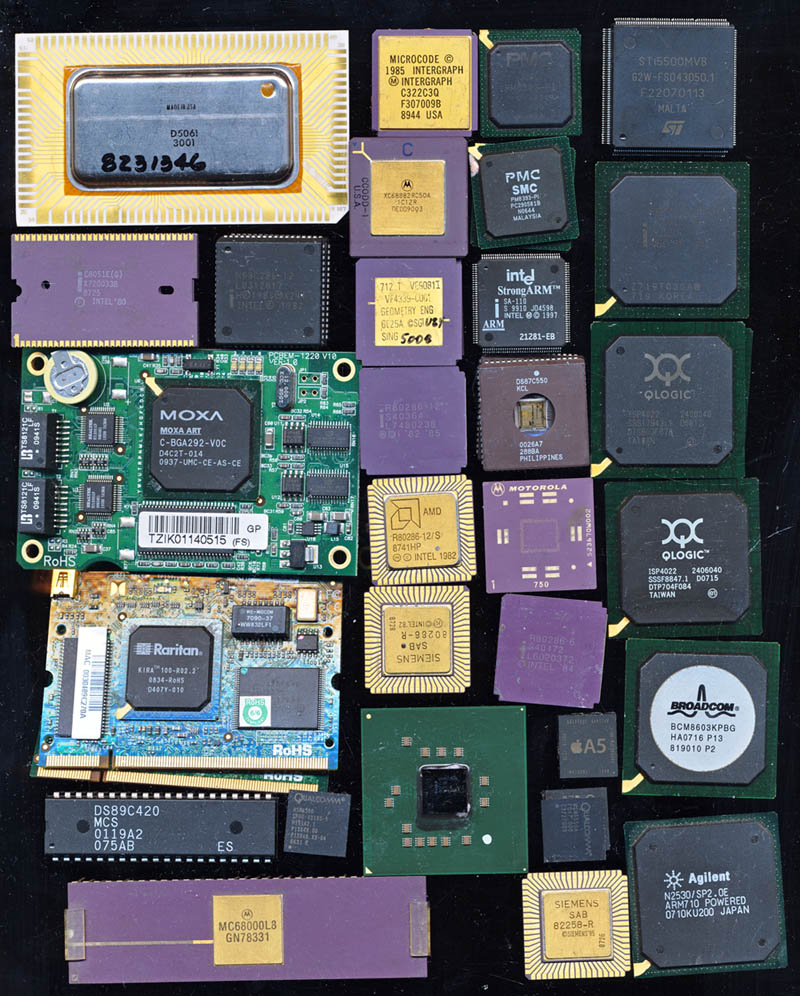
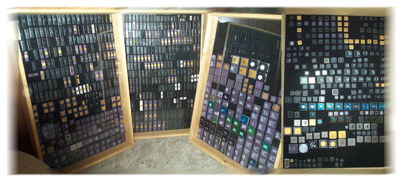
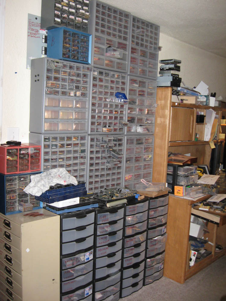
It gets big quickly without proper focus
For some collecting computer chips is a matter of convenience, they have ready access to them (recycling, etc) and are drawn to the fact, that like coins, IC’s have an extrinsic value in their rarity, obscurity, or provenance, but also some intrinsic value in the precious metals they contain. Computers chips also have the benefit that their entire history is contained in a period of time that numbers in the decades, 50 years, shorter than an average human lifetime, contains the current sum of IC history. This can be seen to make the hobby more ‘manageable’ though we will see if Part 2, that this may not be the case.
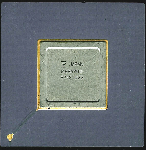
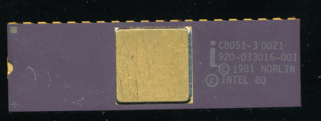
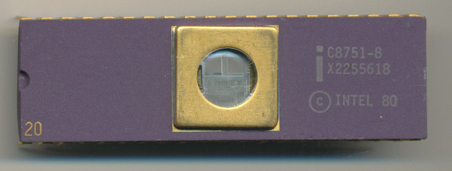
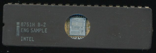
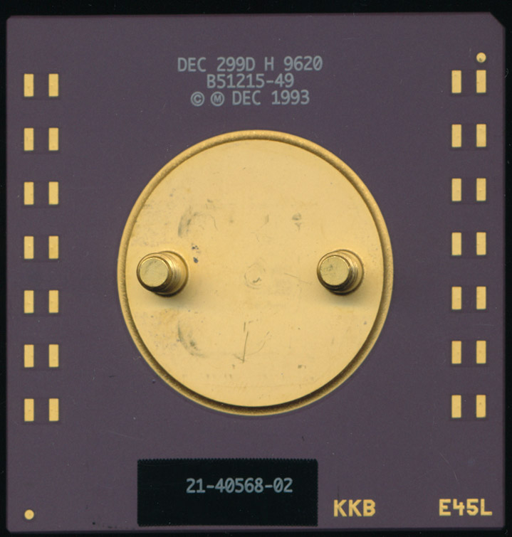
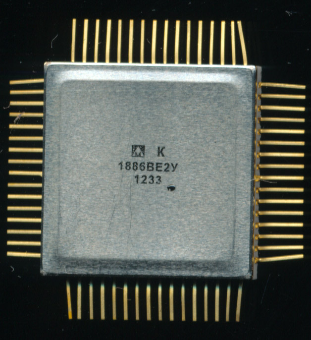
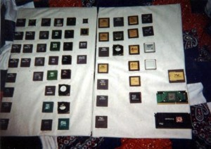
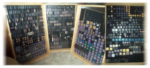
For some, computers chips are shiny, pretty, and look ‘cool’ and thats all thats needed, they collect not for any historical, or technological reason, but for the fact that they like neat looking ‘stuff’. Some collect very large/gold chips only for this reason, or wafers, because they are drawn first, to their beauty.
On the extreme of this is those, as a fellow collector in Romania once told me:
“Basically when I saw in the same place 3 different objects of the same type, my first thought is ” I should start a new collection”
And sometimes, that’s all it takes to get started. Next week we will explore the What of collecting, how to determine what specific type of IC’s you want to collect, and figuring that out early is so important.