Archive for the 'CPU of the Day' Category

April 29th, 2011 ~ by admin

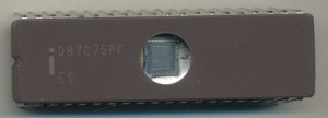
EPROM of the Day: Intel D87C75PF The 8755 gets a boost

Intel C8755A - 1977

When Intel released the 8755 in 1976 and 8755A in 1977 it provided an easy way to interface the 8080 and the 8085 to other components. It was a 16k (2kx8) EPROM with a pair of latched 8 bit I/O ports.  This greatly reduced system chip counts and complexity of board design. The basic 8755A ran at 3Mhz (the later 8755A-2 ran at 5MHz) which allowed interfacing with the 8085AH with zero wait states. The 8755A continued to be used well into the 1980s with many processors (Intel and others)

Intel D87C75PF - 1988 Engineering Sample

By 1988 the 8755A was out of date, its 16k of EPROM space was insufficient for most designs and its power consumption was much higher then contemporary parts. Intel sought to remedy this with the release of the 87C75.  The 87C75 is essnetially a 27C256 EPROM, and 82C55A port expander, and latches combined on a single chip. It was made on Intel CHMOSII-E process which reduced power consumption (from 1.5Watts to 500mW). It ran at a max of 5MHz and the EPROM was bumped up from 16k to 256k. It was designed to interface direction to the 8051, MCS-96 and i188 processors.

Why then do we find so few examples of the 87C75PF?  The late 80’s and early 90’s also ushered in dozens of microcontrollers and embedded processors that had all of the 87C75’s features on chip; larger EPROM on die, more I/O ports, and the widespread use of Flash on microcontrollers effectively made the 87C75PF obsolete.

April 21st, 2011 ~ by admin

Inside the 1802: a Visual6502.org View


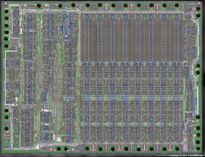
RCA 1802E Die - 20x magnification - Visual6502.org

The talent at Visual6502.org continues.  After imaging and building a complete simulator for the MOS 6502 they did the same for the Motorola 6800 (from which the 6502 was based).

We have sent Visual6502.org several chips and they have now imaged the RCA 1802 that we sent.  What is very interesting is how little marking are on the die, the only that I could see was the number ‘10824.’  This particular chip was dated early 1981 though the 1802 COSMAC was designed in 1976 and was one of the first CMOS microprocessors.  The 1802 had around 5000 transistors (Visual6502 will let us know exactly how many once they are done, and of course what each and every one of them does). For higher res shots and more info see here

March 31st, 2011 ~ by admin

CPU of the Day: MMI 6701 Bit-Slice

In 1974 Monolithic Memories Inc. (MMI) announced the 6701 bit slice device.  At its heart the 6701 is a 4-bit ALU much like the 74181 TTL IC.  The 6701 adds a register, and some other support circuitry on chip making it much more adaptable.  The 6701 has an approximate complexity of 1000 gates (meaning it would replace 1000 gates worth of TTL).  The 6701 was made on a bipolar process and ran at 5.2MHz.  Later versions would up this speed to around 11MHz.

6701D - 1976

The 6701 continues on until around 1980 by which time the AMD 2901 bit-slice processor had come to completely dominate the market.  The Soviets however cloned/modified the 6701 as the 1802VS1 through the 80’s and into the 1990’s.

Posted in:
CPU of the Day

March 17th, 2011 ~ by admin

Chips of the day: TI TMS320E The tale of the two dies

Its fairly common for a manufacturer to make several devices out of a single actual die.  Just disable part of the die, whether because its faulty, or not needed, or simply do not connect the pins to that feature.  Intel did this a lot with the Celeron, and PIII line, disable some L2 cache on a PIII and you get a Celeron.  Today it is done with multi-core processors.

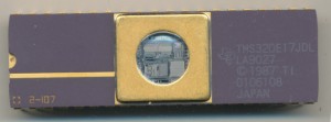
TI TMS320E17JDL

Using a common wafer for several products saves a large amount of money, no need for a second mask set, and testing systems.  Here we have a Texas Instruments TMS320E17JDL.  The TMS320 is the industry standard in DSPs (Digital Signal Processors). The E17  from 1990 runs at 20.5MHz has a 4K EPROM, 256 bytes of RAM, and a pair of serial ports.  You can see the large sections of the die devoted to the ROM, RAM, and MAC (Multiply and Accumulate).

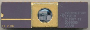
TI TMS320E15JDL

This is the TI TMS320E15JDL.  It is the same basic DSP core as the E17, it includes the same 4K EPROM, the same 256 bytes of RAM and the same MAC unit.  It has some I/O ports tasked with doing different things, but thats a relatively minor difference.  The big difference is the E15 lacks the 2 serial ports of the E17.  You can see on the die where that hardware does not exist, its a large black spot, void of any circuitry.  A very interesting and unusual occurrence.

TI either used a completely different mask for the E15, or they simply chose to not expose that small part of the mask.

Tags:
,

Posted in:
CPU of the Day

March 6th, 2011 ~ by admin

CPU of the Day: NS87P50R-6: Piggyback CPUs

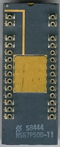
National Semiconductor NS87P50D-11

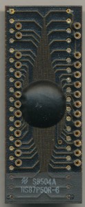
National Semiconductor NS87P50R-6

In the 1980’s most high-volume microcontrollers were OTP (one-time-programmable) or were factory programmed (Mask ROM).  This made developing code for them a bit tricky.  Some companies made lower volume version with an onboard EPROM, such as the Intel 8751.  Other designs this was not practical so another solution had to be found.

The most common solution became the ‘piggyback’ package.  The CPU would reside on a ceramic (pictured on the left) or organic (on the right) package that had a socket on top of it for an EPROM.  This provided an easy way to develop code for the processor, and EPROMs could be stopped out and erased at will.  Obviously these ‘piggyback’ parts were not intended for production use, their cost would be much to high for that.  They were made in relatively small quantities solely for engineering and prototype work.

This National Semiconductor NS87P50R-6 is a 6MHz MCU.  It includes a 24-pin socket on top that supports up to a 32k EPROM (2758, 2716 or 2732).  The other group of 4 pins on top are yet another feature.  It would be cost prohibitive to make a separate development device for each member of the MCU family so the 87P50 can be told to emulate several.  It can emulate a 8048, 8049, or if all jumpers are removed, the 8050. (The only difference in these is the RAM size, 64bytes, 128bytes, or 256bytes for the 8050).  The NS87P50R-6 is in an organic package, the die is actually placed directly on a circuit board, and covered in a black epoxy.  This is rather less expensive then the NS87P50D-11 ceramic and gold version, though is not as tolerant to heat.

If you have ever taken apart a cheap consumer electronic device, you will likely find a black ‘blob’ on the circuit board.  Thats a die, and usually the microcontroller of that device.  ID’ing it is next to impossible without acid and a microscope however.

National Semiconductor was not the only company to use this type of design.  Zilog and Synertek used it for the Z8 series, Hitachi for the HD6301, Mostek for the 3870 and most all other companies that made a MCU int he 1980’s.

Tags:
,

Posted in:
CPU of the Day

January 24th, 2011 ~ by admin

IBM’s Server Processors: The RS64 and the POWER

IBM POWER1 Data Cache circa 1990 - 30MHz

IBM in the late 1990s was making a wide variety of processors, from the Cyrix Design 6x86MX, to fab work for AMD on the K6, to the PowerPC line used in Apple computers.  Most of these processors were low margin designs for the consumer market.  What IBM is best known for, and best at, is server and workstation processors.  The kind of processors you will find by the thousands in Top 500 Supercomputers.

There were three distinct architectures IBM used in this market.  The POWER (Performance Optimization With Enhanced RISC) processor originated in 1990 as a new deign for IBM.  IBM also was working on with Apple and Motorola in a consortium known as AIM to design a PC based processor architecture, loosely based, or inspired by, POWER.  This became known as the PowerPC.  IBM also was looking for a solution to replacing their old AS/400 CISC based computers.  A processor architecture to smooth the transition from CISC, to full on RISC was needed. A subset of the PowerPC design was developed with added instructions from the POWER2 and AS/400 called PowerPC-AS.  The first CPU to use this architecture was the A10, released in 1995 at 77MHz
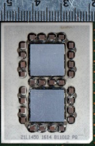
IBM RS64 IV 600MHz Dual Core - 2001

The RS64 line implemented the PowerPC-AS architecture and was initially released in 1997.  RS64 designs were focused mainly on transaction processing and other integer intensive applications.  Their floating point performance was not as good as the POWER architecture.  Debuting at 125MHz with 128kb of L1 cache, and 4MB of off chip L2 cache.  By 2000 IBM had continually improved upon the RS64 architecture, as well as fab processes.  The RS64-IV, the final RS64 processor, was released at 600MHz and topped out at 750MHz.  At the time the POWER line (now at the POWER3) has stagnated, the RS was able to clock twice as fast, and at less power (15W per core)
POWER3-II 375MHz - 2000

In 1998 IBM released the POWER3, the third generation in the POWER line, and the contemporary to the RS64-IV.  The POWER3 essentially merged the full 64-bit PowerPC instruction set into the POWER line.  Initially it ran at 200MHz with 96kb of L1 cache, 16MB of off chip L2 cache. It was manufactured on a hybrid 0.35/0.25u process. In 2000 IBM released the POWER3-II, a process shrink to 0.22u, with other enhancements, that brought the POWER line up to 450MHz.  Still the POWER3 languished in pure speed (at least in integer) against the RS64-IV.

Having two independent processor lines is extremely expensive to maintain.  Support costs, software costs, R&D, etc all were double what they would be with a single unified architecture.  In 2001 IBM released the POWER4 and discontinued the RS64 line.  The POWER4 merged the PowerPC (and POWER) instruction sets with the PowerPC-AS instruction set of the RS64.
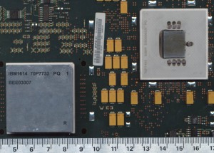
IBM POWER4+ 1.2GHz - 2004

Now IBM had a single processor for both the RS/6000 line and the AS/400 line of computers.  The POWER4 was also an incredible boost in speed and now featured 2-cores on one die (the first non-embedded processor to do so).  Even the initial version did 1.1GHz.  L2 cache size was decreased to 1.4MB but moved on die.  L1 cache remained at 96kb.  To compensate for the reduced L2 cache size IBM added a 32mb off chip L3 cache.   The POWER4+ would eventually hit 1.9GHz.  In the picture on the left the 32MB of L3 cache is the large white chip in the upper right, while the dual core CPU is in the lower left.
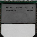
POWER5 1.65GHz - 2004

In 2003 IBM further enhanced the POWER line and released the POWER5 processor.  Again a dual core processor running at 1.5-2.3GHz.  The POWER5 increased the on chip L2 cache to 1.9MB and moved the L3 cache on chip (though a separate die, like the Pentium Pro).  The L3 cache was also increased to 36mb.  As with the POWER4 the POWER5 was also offered in larger MCMs that integrated 4 processor dies, and 4 36mb L3 cache dies onto a single, large, MCM.  IBM has an excellent, in depth article on the differences of the POWER4 and POWER5 here.  IBM continues to develop the POWER line and currently is shipping system based on the 4GHz+ POWER7 processor.  The POWER8 successor is under development.

Posted in:
CPU of the Day

January 16th, 2011 ~ by admin

CPU of the Week: Intergraph Clipper C4 MCM


Fairchild developed the Clipper architecture in 1986, and sold it to Intergraph in 1987.  The design never enjoyed wide success and was only used in systems made by Integraph, as well as some by ‘High Level Hardware.’  The deign itself was RISC like and competed mainly with the Sun SPARC processors.

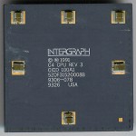
The final version was the C400 which was released in 1993 (preceded by the C100 and C300). Presumably there was a C200 but I have not seen any documentation on it.  The C400 ran at 50MHz (like the C300) and actually consisted of 3 separate chips. The CPU, the FPU and the CAMMU (Cache/Memory Management Unit).  Intergraph developed their own version of UNIX called CLIX to run on the clipper, and demonstrated a version of Windows NT that ran on the C400 as well. Ultimately the lack of software support, and the slow adoption killed the Clipper.  While Intergraph was designing the C5, Intel assured them a good supply of processors, and this convinced Intergraph to cancel the C5.

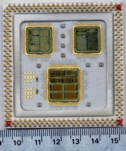
Intergraph C4 MCM

It was also available as a MCM (multi-chip-module) incorporating all three dies in a single ceramic package.  This is one of the nicest looking MCMs I have seen, unfortunately the bottom plate was missing when I got it, but the dies are at least visible.  I unfortunately am not sure which die is which so if you know, let me know.

Posted in:
CPU of the Day

December 12th, 2010 ~ by admin

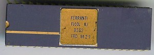
CPU of the Day: Ferranti FBH 5092 – The F100L MCM

In the 1970’s the British electronics company Ferranti was commissioned by the Ministry of Defense to develop a processor for military applications.  The desire was for something along the lines of the American MIL-STD-1750A processor.

Ferranti F100L - 1986

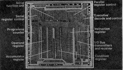
In 1977 Ferranti released the F100-L 16-bit processor. It was made using Bipolar technology (rather then MOS) so it could easily hit speeds of 8MHz (albeit getting rather warm in the process).  The F100-L was one of the first 16-bit processors made (along with the National Semiconductor PACE). The processor contained over 1500 gates and was made using  collector diffusion isolation (an enhanced Bipolar design) and was produced with 3.5 micron features. The die itself occupied 60mm^2.

Ferranti F100-L Die

The F100-L was designed to handle real time data quickly and efficiently (time critical processing of signals and information is always one of the key requirements of a military specific design).  It however was not as adaptable or flexible for use in standard computing environments.  Ferranti tried to sell it commercially with only limited success.  It ended up in some of the same uses as the Signetics/SMS 8X300 series of processors.

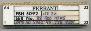
Ferranti FBH5092 - F100-L Hybrid Module

Ferranti also made the F100-L in a Hybrid, or MCM (Multi-Chip-Module) that contained a F100-L processor, a F101-L Multiply/Divide unit (a simple FPU), clock generators, and a pair of F112-L Data Interfaces to act as buffers.  All of ths was packaged in a single 64 pin DIP.

Tags:

Posted in:
CPU of the Day

October 11th, 2010 ~ by admin

Soviet Beauties: Processors from behind the Iron Curtain

The Soviet Union’s electronic programs were mainly focused on copying and cloning Western devices.  Either by simple theft, or painstaking reverse engineering.  They made clones of devices such as the Intel 8080, and the AMD 2901 as well as simple TTL.  The Soviets also made many single and multi-chip versions of the venerable DEC PDP-11 computer system.  Many of these have no Western analogs, they were pure creations of the Soviet industry.

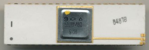
Soviet Kvantor 580VM80 - Intel 8080 - Milspec

While Western chips rapidly transitioned into mostly black plastic by the 1980s the Soviets did not.  The 8080 above was made in 1991 though looks like something from the 70’s. Black plastic is cheap, and easy to make, but it isn’t great looking. The Soviets on the other hand made some of the best looking (if not always functioning) processors of the time.

Soviet J-11 Missing the chips

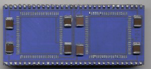
Here is just the substrate (its a non finished example) of a Soviet clone of the DEC J-11 CPU. Not often do you see a brilliant blue processor.

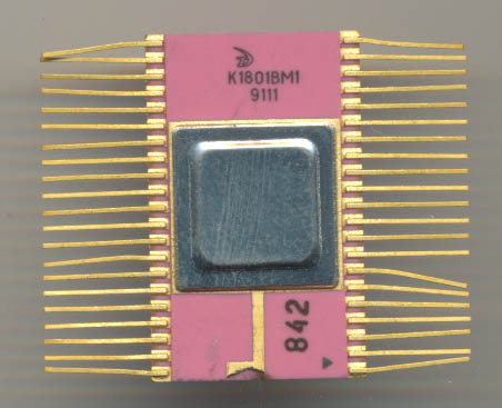
Soviet Angstrem K1801VM1

This is a nice pink ceramic Soviet PDP-11 5MHz CPU. Again this was made in 1991.  Its a form of surface mount package that was used extensively for industrial and military designs.  Just as the PDP-11 was used by the American military throughout the 70’s and 80’s. the Soviets used it (and now Russians) in todays times.

Soviet era CPUs are very interesting to collect.  Each state run factory had their own logo which was typically (but not always) put on the chip. Many part numbers were made by more then one factory. Most chips have a western analog, but not all.  Soviet chips also were ever so slightly different sized then Western ones. The Soviets used a pin spacing of 2.5mm where as the West used 0.1″ (2.54″), rather noticeable on a 40 pin DIP. Reading/translating some of the Cyrillic  based characters can be a chore but really when you get to see things like this…

Electronika J-11 - Image courtesy of iguana_kiev

Can you really complain?

April 9th, 2010 ~ by admin

Cyrix MediaGX: From Cyrix to AMD – A bit a History

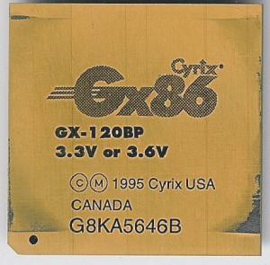
On February 20th of 1997 Cyrix announced the MediaGX processor, running at speeds of 120 and 133MHz. By June of that year they were up to 180MHz as production was ramped at National and IBM (see press release). These processors were based on the Cyrix M1 (5×86) architecture and integrated basic graphics, and audio functions. They were sold as a ‘PC on a chip’ for budget applications, with a bit of a budget performance.

Early MediaGX Marked Gx86 120MHz circa late '96

In October 1997 Cyrix announced plans for the Cayenne cored MXi, a follow on to the MediaGX. By 1999 National Semiconductor had made some samples of it, but thats as far as it got. This was also when National Semiconductor bought Cyrix, effectively ending Intel’s lawsuit against Cyrix over x86 licensing as National held an x86 license. The Media GX was bumped to 200 and 233MHz and MMX support was added.

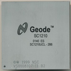
National Semiconductor Geode 266MHz circa 2001 Sample

Read More »