May 27th, 2013 ~ by admin
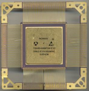
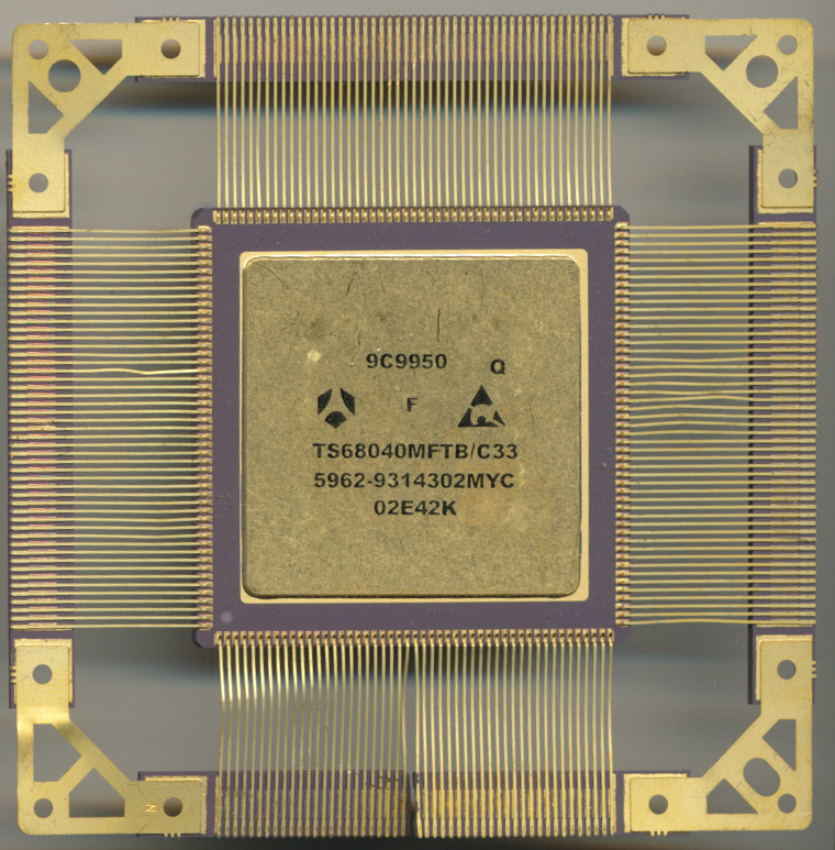
Thomson TS68040MFTB/C 33 5962-9314302MYC
Since its Memorial Day here in the United States, the CPU for the day needed to be something mil-spec. This is a very nice Thomson-CSF (part of STMicroelectronics) 68040 processor. The 68040 was released in 1990 by Motorola and was the first of the 68k line to include a full FPU on chip (as opposed to using the 68881/2).
This Thomson part was made in 1999. It is full military temp range (-55 -> 125C) with MIL-STD-883 Class B screening running at 33MHz. Its in a fairly rare (and available by special request only) ‘flat tie bar package’ This is similar to the more common ceramic quad flat pack (CQFP) but the leads are contained and supported by tie bars on the ends. These tie bars are physically attached to the board offering a very strong mechanical support for the processor in environments where high vibrations or higher then normal g-forces may be encountered. The life of a soldier is not an easy one, so electronics must be made to support them, and not fail.
May 21st, 2013 ~ by admin
8-bit 8MHz w/ ADC and 16K EPROM
One of the most well known microcontroller families is the Intel MCS-51. It was introduced in 1980 and is still being made in many many forms. It, however, is not the only popular 8-bit microcontroller. Motorola made many microcontroller versions of the famous 6800 CPU. Namely the MC6804 and the still in production 68HC05 series.
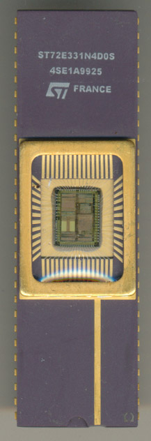
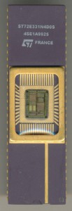
ST, which was formed by the merger of SGS of Italy, and Thomson of France, also makes a wide range of 8-bit microcontrollers which are very popular and widely used. The ST7 microcontroller is a 8-bit Von Neumann architecture (shared address/data bus) MCU. It is a serial accumulator design (so all operations occur in the accumulator, rather than in a wide set of registers like the 8051). The ST7 was introduced in the early 1990’s as an upgrade to the ST6 Family of microcontrollers. The ST7 added more high level programming support, and better interrupt handling. The ST7 provides higher performance then many competing architectures and in various performance tests such as IRQ handling, returns, instruction execution times etc, it even beats the venerable 80C51.
Both the ST6 and ST7 families are based on the Motorola MS680x microcontroller family. The ST6 closely resembles the 6804 and the ST7 is upwards code compatible with the MC68HC05 (assembly level translators exist to port the raw code). The ST7 has 63 instructions and the 6805 has 62 (depending on version). It is not an uncommon practice for one MCU to be based off, or even compatible with another. It provides more familiarity for programmers and design engineers. What really sets a MCU apart is the peripherals that surround the core, and its operating parameters. The ST6 and ST7 are both highly respected for their ESD protection and high noise immunity. These features were both carried over into the ST8M family that was introduced in 2008 to replace the aging ST7. The ST7 can be found in many applications such as automotive appliance control, motor control, and other embedded systems that most people forget are run by a processor.
May 16th, 2013 ~ by admin
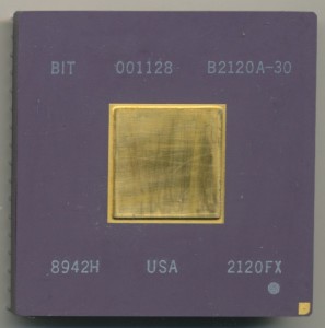
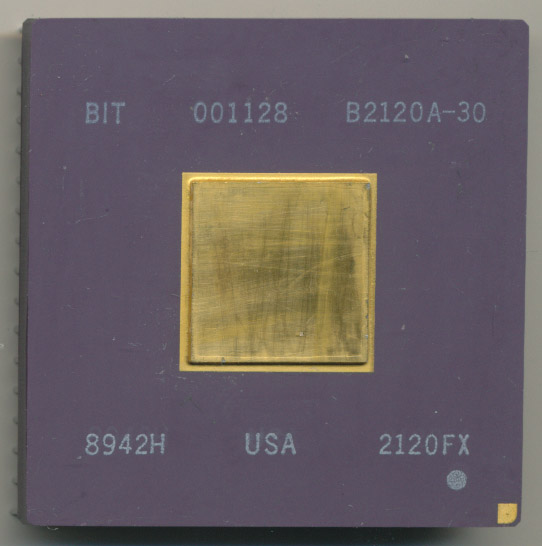
B2120A Floating Point ALU 1989 33MHz
Bipolar Integrated Technology Inc. (BIT) was founded in 1983 in Beaverton Oregon by former Floating Point Systems, Intel, and Tektronix engineers. Their goal was to develop fast floating point processors based on a bipolar process (rather then the more common NMOS and CMOS of the time. The bipolar process is used to make TTL, and ECL type products, and had been used in several previous processors, including the AMD 2901 and the SMS300 (Signetics 8X300).
The B2120 was part of a complete floating point chip set that was released in 1987. the B2120 handled all the ALU functions, while the B2110 was the multiplier. It was designed by Bob Elkind who was one of the original employees of BIT and oversaw the development, layout, and packaging of most of their early products. The B2120 was a TTL compatible device while the B3120 and B3110 made using ECL 10KH instead. Both were made using Bipolar’s proprietary P111 1.2 micron process. The B2120A-30 had a typical cycle time of 30ns, giving it an effective clock rate of 33MHz.
In 1990 BIT introduced the B2130 (TTL) B3130 (ECL 10KH) and B4130 (ECL 100k) which were 100MHz single chip versions of the 2110/2120
BIT would later make a SPARC chipset called the B5000 (which at 80MHz was the fastest processor of its time) and a follow on version called the B6000. Both were made using ECL. Reliability problems and the eventual catchin up of CMOS in speed led to their demise, and in 1996 BIT was purchased by PMC-Sierra (who ended up consolidating a lot of 80’s and 90’s companies).
May 6th, 2013 ~ by admin
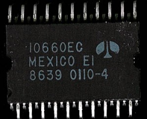
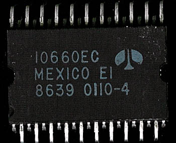
Rockwell 10660EC PPS-4 – 1986
The Intel 4004 processor gets much attention for being the ‘first’ processor, however, there were others. The Rockwell PPS-4 was introduced in 1972, making it one of only 4 processors of the time (IMP-16 from National Semiconductor, Intel 8008 and Intel 4004 being the others.
The original PPS-4 came in a 42 pin Quad Inline package, compared to the 4004s somewhat limiting 16 pins. A complete system could be built using 3 chips, a 10660 (later the 12660) PPS-4 processor, a ROM, and a clock generator (10706). The PPS-4 was manufactured on a metal gate process (vs the silicon gate process of the 4004). It required a single -17VDC power supply and ran at 256KHz.
In 1975 Rockwell introduced the PPS-4/2 (aka the 11660). The ‘/2’ denoting the 2 chip version of the PPS-4. The clock generator was now moved onto the processor itself, and a memory/IO chip (part # A17xx) that provided 2048×8 bits of ROM 128×4 bits of RAM and 16 1 bit I/O ports. Clock speed was 200KHz, slightly less than that of the 3 chip PPS-4.
Rockwell was not done with the PPS-4. In 1976 they released the PPS-4/1, which was a single chip microcomputer version, integrating ROM onto the processor so that a system could be built with one chip. The standard version (the MM76) had 64×8 bits of ROM and 48×4 bits of RAM. Clock frequency could range from 40KHz to a blistering 120KHz. The PPS-4/1 was compatible with peripherals of the newly released PPS-8 as well. Additional versions were made including:
MM75: Reduced I/O 28 pin version
MM76E: Extended memory 1024x8bits of ROM
MM76C: Included a high speed counter and expanded I/O in a 52 pin package (140KHz max speed)
MM76D: Includes a ADC 52 pin package
MM76L/EL: Low voltage/low power version (-11 – -6.4 volts vs -15 of the standard parts)
MM77: 1344×8 ROM 96×4 RAM
MM78: 2048×8 bit ROM 128×4 RAM
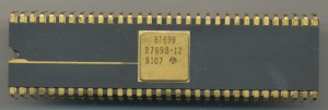
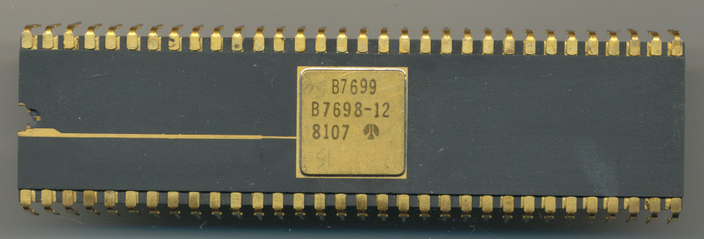
Rockwell B7699 PPS4/1 Low power External ROM Development device – 1981
A7699: Development version without on board ROM – requires external clocking
A7698: Development version without on board ROM – Can use internal clock
B769x: Development version for the MM76L/EL Low power versions
Unlike the Intel MCS-4/40 the Rockwell PPS-4 and its derivatives continued to be made and used well into the late 1980’s
April 7th, 2013 ~ by admin
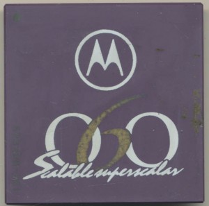
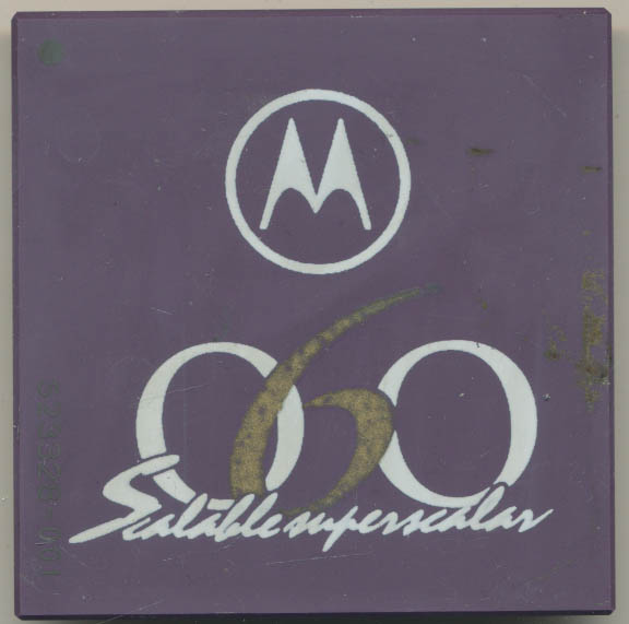
Motorola 68060 Marketing Sample
The Motorola 68060 was the last of the 68k line that was begun in the late 1970’s. The 68k began as the first commercial success of a 32 bit processor. It wen through many upgrades, essentially proving to be worth competition (and likely a better architecture) to Intel’s x86 line. The ‘060 was the first 68k to bring a superscalar architecture. It could issue multiple instructions per clock, in some ways it was better then the Intel Pentium. The 68060 was released in 1994 but never achieved wide success. By the time of its introduction Motorola had thrown most of its weight behind the PowerPC of the AIM Alliance. Eventually the 68060, which was released on a 0.6micron process at 50MHz, would be moved to 0.42 micron and hit 75MHz.
It, unfortunately, suffered the same fate as the 88000 RISC processor, a slow but inevitable fading away. The 68k line (mostly the 68000 core, or its derivative, the CPU32) lives on in many of Freescale’s products.
The chip shown is what is known as a Marketing Sample. These typically were only an empty package, given to sale people and distributors as gifts or sales aids. They typically feature a flashy logo, more color, and often, like this one, a sales pitch. ‘Scalable Superscalar’. It seems that the 68060 proved less salable then it was scalable.
April 2nd, 2013 ~ by admin
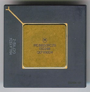
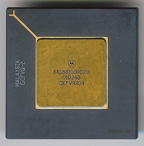
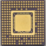
MC88100 20MHz – 1992
In the late 1980’s Motorola was developing a full 32-bit RISC processor from the ground up. Initially called the 78000, it was renamed the 88000. The first implementation of the 88000 Instruction Set Architecture was the 88100. It included a FPU and integer unit but required a separate chip (the 88200 CMMU) for caching and memory management. Typically 2 of the 88200s were required (one for instruction cache, one for data, 16kb of cache each). A 64lb cache was also available called the 88204. Made on a 1.5u process the 88100 contained 165,000 transistors while the CMMU chips contained 750,000. Each chip dissipated 1.5Watts at 25MHz. Prices in 1989 were $494 for the CPU and $619 each for the CMMUs. A complete system of 3 chips would be nearly $2000. Not exactly competitive pricing.
The initial, and biggest, customers for the 88000 were to be Apple, and Ford Motor Company, an unusual combination to say the least. Apple invested in the 88000 to be the replacement for the 680×0 processors it had been using. Ford was looking to replace the Intel 8061 processors (from which the MCS-96 MCUs were developed) that had run their EEC-IV engine computers since the early 1980’s. Motorola (as well as Toshiba) had been second sourcing these for Ford for sometime. Ford based its choice on the 88100 based ECU on the assumption that Apples adoption of the 88100 would guarantee good software and compiler support. If Apple stuck with it that is..
Read More »
March 22nd, 2013 ~ by admin
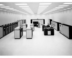
IBM System/370 – 1970
IBM introduced the 12.5MHz cabinet sized System/370 in June 1970 as an evolution of the System/360 from 1964. These systems formed the entire base of IBM’s mainframe business. Today’s System z, itself an evolution of the original System/360 and 370, can still run many of the original programs, unmodified, from 50 years ago. This is a testament to 2 things, the wide adoption of the IBM systems, and the forward thinking of IBM. Even the original System/360 from 1964 was a full 32-bit computer. Single chip processors did not embrace 32 bit architectures until the very early 1980’s (Motorola 68k, National 32k, etc).
In 1980 IBM sought to make a single chip version of the 370, in an effort to make a version that could be used for desktop type computers. This was to become the Micro/370. There were 2 distinct products to come out of this goal that are widely confused and debated. The first became the PC XT/370, an add in card(s) for an IBM PC to give it the capability to run System/370 software. Later another version was developed called the Micro/370 as a single chip solution.
The PC XT/370 began as an experiment, a test bed implementation of the System/370 in a microprocessor environment. The goal was not to rebuild the 370 from the ground up (that would come later) but to merely implement its instruction set into an existing design. The base processor had two main requirements: it had to be 32 bits, and it had to be microcoded. IBM’s engineers in Endicott, NY selected the then very new Motorola MC68000 processor as their basis. It was one of the only 32-bit designs at them time so that no doubt helped in the selection process.
Read More »
March 16th, 2013 ~ by admin
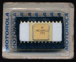
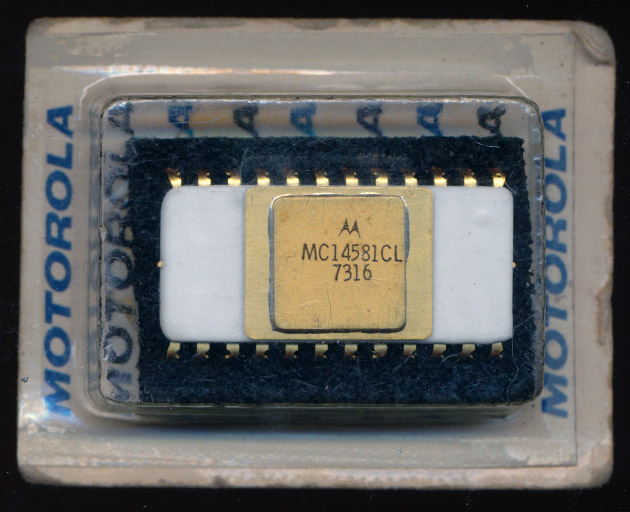
Motorola MC14581CL 4-bit ALU – 1973
At the heart of every processor is an ALU, an Arithmetic Logic Unit. It is what does the addition, subtraction, compares, and other logic function on the bits we call data. Add some memory for registers, stack, and program control and one has a basic processor, or bit slice processor. In the 1970’s and even the 1980’s many systems still implemented their ‘processor’ in discrete logic. The 74181 (TTL), 10181 (ECL) and 14581 (CMOS) were the heart of many of them. The ‘181 could handle any of 16 arithmetic and logic functions on a pair of 4 bit words.
The Motorola MC14581CL was the first of the CMOS ALU’s. This example was made in early 1973. CMOS itself was only patented a few years prior (1967) and didn’t see extensive use in processors until the mid 1970’s (RCA 1802) and most other processors in the 1980’s. Remarkably, after 40 years, its still in its original package.
March 10th, 2013 ~ by admin
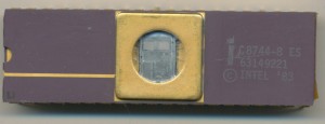
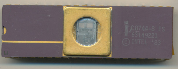
Intel C8744-8 Engineering Sample – Early 1983
In 1980 Intel released the MCS-51 family of microcontrollers, a design that would go on to become one of the pillars of the 8-bit MCU market. Initially the family consisted of the 8051, which included 4KBytes of on-chip ROM (or UV-EPROM in the case of the 8751) and 128 bytes of RAM as well as the 8031 which did not include the ROM, all program memory was off chip.
The 8051 was a wild success with Intel struggling to meet demand. Intel did not have the fab capacity to produce both the 8051, and the very in demand 8088 (thanks to IBM). In 1984 Intel opened a new fab in Albuquerque, New Mexico to build other chips, freeing up production space in the California fab for more 8051s. Even so, an $8 8051 was routinely scalped for over $200 on the grey market and waiting periods of up to a year were common in order to receive orders, with many companies on allocation. Intel licensed the design to both AMD (who built a fab in Austin to make it) as well as Signetics in an effort to keep up with demand. The hardest to get part in the industry, was the 8051 from 1983-1984.

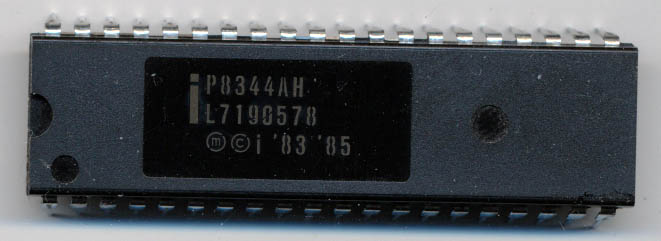
P8344 – A ROMLess 8044, so essentially an 8031 + SDLC controller.
So in the midst of this insatiable demand for an MCU that they did not have the capacity to produce, Intel releases the RUPI-44 (Remote Universal Peripheral Interface). The RUPI-44, also known as the 8044, is an 8051 with an additional 64 bytes of RAM and a full serial communication co-processor on die. Specifically it was an 8051 that handled the SDLC (Synchronous Data Link Control) protocol in hardware. Intel had an SDLC controller, known as the 8273, but it was limited to 64kbps, the 8044 could handle data transfers of up to 2.4Mbps due to the 8051 core’s high speed and close coupling of the serial controller.
SDLC was developed in 1975 by IBM and was generally used as a way for mainframes to communicate with various peripherals and terminals. It supports error correction and multi-point, point to point, and loop connections. In 1979 SDLC was standardized as HDLC (High-Level Data Link Control) which the RUPI-44 also supports. While popular in the 70’s and 80’s its use has faded out, though it achieved some long lived use in Europe running the Intel derived BITBUS protocol well into the 90’s.
Read More »
February 27th, 2013 ~ by admin
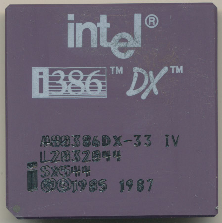
 In coin collecting often times an example is valued not because of its perfection, but because of its imperfections. An off-center print, the obverse being printed upside down, or the double strike, where a coin doesn’t get cleared form the die and gets hit twice.
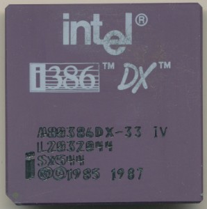
Such appears to be the case with this Intel A80386DX-33. It clearly went through the engraver twice. A similar example (from the same exact lot) is fine, so clearly this one, made in early 1992, was a mistake that was not caught. I have seen mis-aligned prints, off center etc, but this is the first example i have seen that was engraved twice. It is interesting that even within the same lot, the spacing of the markings varied somewhat. Notice that on the right side of the chips the sets of markings line up but they diverge towards the left. It appears the stepper motors moving the tooling or the chips were a bit sloppy or out of calibration.
Have you seen any other double engraved comments? Let us know in the comments.