Archive for September, 2021

September 28th, 2021 ~ by admin

The RCA Solid State Technology Center (SSTC)

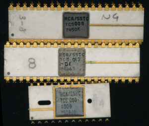
TCS008 Adder – TCS017 FPU Control and TCS060 Shift Register – 1974-1975

Today most chips we use are made in CMOS (Complimentary Symmetrical Metal Oxide Semiconductor), which is a process using both p-type and n-type MOSFET transistors.  It was invented back in 1963 by Fairchild, but was commercialized by RCA in 1968 with the introduction of the CMOS based 4000 series of MSI logic devices.  These were basic IC’s with such things as NOR gates, Adders, Flip flops and the like.  A CMOS equivalent to TI’s popular TTL based 7400 series.

RCA also made a series of computers in the 1960’s (to compete with IBM) as well as other electronic products. including many for the US Air Force, NASA and US Army.  In 1970 RCA created the SSTC (Solid State Technology Division) in Somerville, New Jersey to develop CMOS processes (and Silicon on Sapphire versions) into more commercial products. At the time most IC’s (outside the 4000 series) were made in PMOS or NMOS, CMOS was considered too slow, despite is lower static power usage and high noise immunity.  SSTC was to develop processes, standard, and eventually devices, that RCA could then commercialize and/or use in their other products (such as their computer line, radios, and military products).  It was out of this project that the famous COSMAC processors (CDP1801 and CDP1802 line) came from.

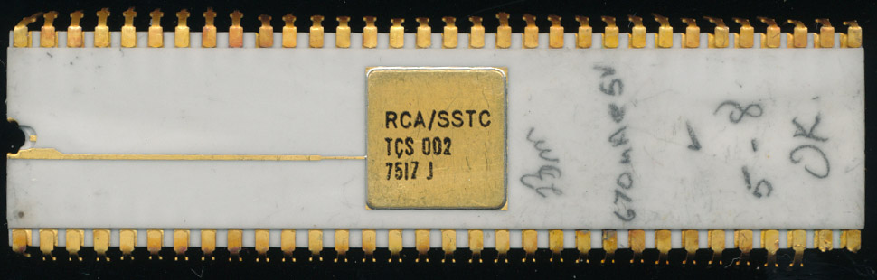
TCS002 16×16 Multiplier 200ns – Note the hand written characterization markings – 670uA @ 5V

SSTC also made a series of essentially standard test devices.  These were based on a common cell architecture (more common in ASICs today) with a series of chips made to demo what was possible with the CMOS-SOS (CMOS on Sapphire) process.  These ‘standard’ IC’s would then be used in various demo products for potential customers.  The most interested customers at the time were the US Air Force and NASA.  The RCA CMOS process allowed for a great power savings, and especially when built on a sapphire substrate, exhibited a high tolerance to radiation, useful for the then rapidly expanding satellite/space market.

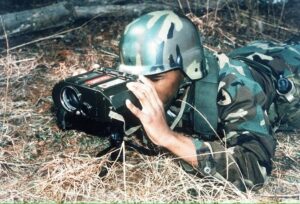
AN/GVS-5 Laser Range Finder – 1970’s. They were huge, but very impressive for their day

The first of these chips were made in 1974-1975 and were made with a 7 mil (178micron) standard cell height, on a 20 micron process.  Versions were also made with a 5 mil (127 micron) size, specifically for the military market.   These were not typically commercially available devices, but used internally for test, evaluation, and to build specific products, though the technology used for them was often turned into generic products.

Below is a list of some of these devices SSTC made. The TCS prefix was used to denote these being made by SSC on a CMOS-SOS process.  A TCC prefix is a standard CMOS process.

Device Function
TCS001 16×16 Multiplier
TCS002 16×16 Multiplier 200nsec
TCS008 8×8 Adder
TCS015 18-bit Reclocking Register with complement select
TCS016 Dual 8 -Bit Position Scaler for Floating Point Applications and Other Binary Division.
TCS017 Floating Point Control for FFT Arithmetic Unit of Arbitrary Radix (Parallelism)
TCS026 Floating Point 2×1 Multiplexer – 163 gates**
TCS027 12-bit Up/down counter (8+4) – 300 gates**
TCS029 Unknown**
TCS030 8-bit Adder = 450 gates**
TCS031 9-bit 4×2 Multiplexer – 150 gates**
TCS032 Adder Multiplexer Control – 166 gates**
TCS039 Multiplier
TCS040 Correlator
TCS043 D/A converter (rad hard)
TCS045 Code Generator
TCS047 Frequency synthesizer
TCS057 9×9 Multiplier (8×8 + sign)
TCS060 Shift Register with Variable Length, Complementing Functions and
Switched Delays. Total Registers = 38 Bits
TCS065 9+9 Adder(8+8 + sign)
TCS074 ROM
TCS130 16K SRAM
TCS151 4K SRAM

**Used to build the NASA 32-bit SUMC (Space Ultrareliable Modular Computer)

These were used in many military products such as the AN/GVS-5 handheld laser rangefinder, a Programmable waveform generator used in FM RADARs, and for the imaging system (digitization and compression of video to be sent) in the remotely piloted Lockheed MQM-105 Aquila drone (yah drones, back in 1975).  The Aquila project was particularly challenging, as the circuitry had to be small enough, and low power enough to fit on a small airframe, yet still handle video compression fast enough that a ground station could receive and decode useful imagery.   This was done with several large hybrid circuit modules consisting of many TCS057 Multipliers and TCS065 Adders.  This was capable of 200-1600Kbps data rates, not bad in 1975.

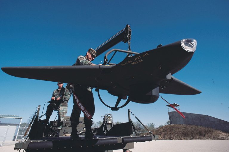
Aquila Artillery Spotting Drone (Lockheed Martin)

Most of the TCS line of components was capable of 10MHz operation while running at 5V, and voltage and clock rate scaled with each other, so they could be clocked lower for less voltage and power usage, or clocked higher at the expense of more power.

It is a bit unfortunately that RCA lost its way in the 1970’s, attempting to became a conglomerate, they became known as Rugs, Chickens and Automobiles (having bought parts of Hertz Rental Cars, a frozen TV dinner company, a carpet company and others).  They were bought by GE in the 1980’s and in 1988 the Solid State Division, with what remained of the SSTC was purchased by Harris Corporation, which continued to make the 180x line of CMOS processors for over 20 years.  If RCA had stayed focused on making CMOS a commercial success, we may have had more and faster CMOS processors nearly a decade sooner.


Tags:
, ,

Posted in:
CPU of the Day

September 1st, 2021 ~ by admin

NEC’s Forgotten FPUs

NEC uPD70108C – V20 CPU – Late 1984

NEC had a cross license agreement with Intel dating back to April of 1976 that allowed each company to make/sell products based on each others patents.  This was particularly important in the 1970’s as having a viable ‘second source’ for your designs was considered critical for it to be viable in the market.  This was especially true for Intel, who wanted to get into the Japanese market. In 1979 NEC began to produce and sell the 8086 and 8088 processors.  NEC wasn’t going to succeed by just being a second source to Intel though, designing their own processors was of great importance.  While producing the 8086/8088 they also began working on their own version, which would be an enhanced 8086/8088 processor.

NEC V30 Die (courtesy Birdman) – 8086 with many enhancements

The result was the rather well known V20/V30 processors of 1984.  These were not just clones of the Intel MCS-86 (though determining this took several court cases and resulted in the Chip Act of 1984).  The V30 had some pretty big differences, notably, internally it had dual 16-bit busses, allowed data to be moved much more efficiently, as data could be moved into and out of a register at the same time (nearly).  It also increased the microinstruction word from 21 bits to 29 bits, added a hardware effective address generator, additional instruction pointers, and a hardware shift/loop counter.  Taking advantage of these features added some new instructions as well, 156 compared to the 8086’s base 133.  The V30/V20 were the beginning of a line of V-series processors.  NEC went on to make  ‘186/188 style processor (the V40/V50) as well as a series of microcontroller versions  (V25/V35 and others).  The V20/V30 were to be supported by a math coprocessor like the 8087 called the upd72091.  Very little info is available on the 72091 as it was cancelled very early on in its design, as by 1984-1985 it was already out of date.  Its replacement was to be a bit more powerful.

Design of the the upd72191 started likely at the same time the V30 was released, around 1984-85, with specifications released in 1986, and plans for chips by 1987.  This chip was in an advanced state of planning, such that many products, including motherboards (such as the Ampro Little Board PC) and industrial controllers designed with sockets for it.  Preliminary datasheets exist, but alas, no chips seem to be found.

LittleBoard PC (Ampro) with support for canceled upD72191 (V40 based)

The upd72191 was made in CMOS and is a bit like an enhanced 80C187 but with support for the V20/V30.  It is fully IEEE-754 compatible (the 8087 wasn’t as the standard wasn’t finished yet) and supports a similar instruction set as the 80C187 (and thus the 80387).  Unlike the 8087 it supports the full set of Exponential, Trig, Logarithmic, and Hyperbolic instructions.  The 8087 was somewhat limited in this, as it was already pushing the limits of what was possible on a single chip at thee time of its release.  The 72191 supports FSIN/FCOS which the 8087 doesn’t and many other functions (its full instruction set could not be found).  The 72191 has a mode pin that selects between interfacing between the V20/V30 and the V40/V50, (as these talked to coprocessors differently) so it was compatible with 4 distinct processors.  The 80C187 could only be used with the 80186 and the 8087 could only be used with the 8086/8088.

upD72191 FPU Block Diagram – 1986ish

Looking at the block diagram of the ‘191 we notice something else, its a dual bus design, much like the V30 processor.  Internally there are a pair of 74-bit busses for the mantissa (fraction) side and a pair of 16-bit busses for the exponent side.  This is a striking difference from that of the 8087 and the ‘187.  The 8087 has a single 16-bit bus for the exponent, and a 64-bit (68-bits into the shifter and ALU) for the mantissa.  There are 3 extra bits for enhanced accuracy, and a extra leading bit that is always 1 for floating point math, giving 64 bits of ‘data’.

The dual bus design makes sense as NEC did the same for the V-series.  Coupled with the right microcode, it can greatly enhance the speed of the FPU.   So why then is the bus expanded to 74-bits for the mantissa?   In the 80187 and 80387 this bus is still only 68-bits.  We look to the design of NECs follow on FPU for the answer.  The upd72291 (and its 32-bit bus 72691 version) are rather different beasts, made for the the V33/V53 x86 CPUs and V60/V70/V80 non x86-CPUs.  We’ll talk about them in more detail later, but they share the same 74-bit mantissa as the 72191, and in this case, the designers wrote a paper on its design.

The FPP [72691] is the only floating point processor that provides the power function xy.  This function (called FPOWER in the instruction set) is difficult to implement not only for its complex definition but also for sufficient accuracy. The equation Xy = e(y*logeX)
does not give good accuracy because the accuracy error of the log function is augmented by the exponential function.  The FPP solves this problem by providing a 74-bit data width for the mantissa data bus.

Being as the 72191 was canceled, the ‘291/691 would in fact have been the only FPU to support this in hardware, but it seems it was first implemented on the ‘191.  The solution only works well for larger (greater then 32) values of y, otherwise iterative multiplication is used, but where it can be used it greatly speeds up the calculation.

When the 72191 was canceled NEC thoughtfully provided a single chip solution called the upd9335C for allowing an 8087 to be interfaced to the V40/V50 processors which, like a 186, used a HOLD/HOLDACK bus release protocol instead of the 8086/8088s (and V20/V30s) REQUEST/GRANT.  For applications using a V20/V30, an 8087 could be used directly.

NEC upD70632R-20 20MHz V70 Processor

In 1989 NEC released the next of the V-series, the V60, V70 and later the V80 processors.  These were a departure from the previous in that they were no longer based on the x86 architecture, but rather a completely new ISA (though the V60 and V70 had a V20/V30 emulation mode).  These were full 32-bit designs, and were Japan’s first widely available 32-bit processors.  Of course with a new processor comes the need for a new FPU and NEC had not one, but 2 FPU options for these.  The upd72291 and upd72691 are based on the same design, but with some major feature differences.  The 72291 is designed to work with processors that have a 16-bit data bus such as the V60.  It also could be used with the older V33/V53 x86 designs.  Internally it has eight floating point registers and supports all your typical floating point functions as well as vector math functions.  The upd72691 is designed for 32-bit data paths, but adds a bit more…

NEC updD72291R-16 FPU

In addition to expanding the register set to 32 FP registers, the ‘691 also added a complete suite of matrix  math functions. The ‘691 was made on a 1.2u CMOS process and contained 433,000 transistors. (nearly 50,000 MORE then the V60 processor) Running at 20MHz it was capable of around 6.7MFLOP and supported 24 vector/matric instructions as well as 22 mathematical functions.  Like the 72191 it had a 74-bit mantissa datapath, but expanded the exponent path to 17-bits to support double extended precision number formats. It is a highly microcoded design using a 3072 word (43 bit word) microcode ROM, 20% for vector/matrix, 37% for arithmetic, and the rest for exceptions handling and other house keeping instructions. Interestingly, these microps themselves encode additional instructions that NEC call nano-ops, these controlled just the ALU operations of the instruction (the rest being bus control and sequencing).  These nano-ops were stored in a 256 word x 74-bit Nano ROM (only 120 words were used, the rest for potential expansion). This was the last of the line of NECs dedicated FPUs (excluding the few MIPS FPUs they made).  Its a bit ironic that it seems they canceled as many designs as they made.

…but perhaps they didn’t?

Read More »

Tags:
, , , , ,

Posted in:
CPU of the Day