Archive for June, 2021

June 27th, 2021 ~ by admin

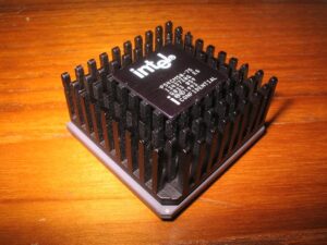
Navy Hydrophone Noise Canceller: Weitek 3332 Floating Point Based DSP

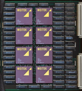
Navy 55910 ASSY 0120811 Eight Channel DSP – Serial #1

I got these boards some time ago, hoping to be able to figure out more about them but alas, information is very sparse, but they are such good looing boards, with impressive technology for the day, I had to post them

These boards came out of a US Navy system labeled “Hydrophone Noise Canceller”  which seemed to be part of SONAR test system at a University.  These date from the late 1980’s to the early 1990’s. The system was comprised of 16 boards, 12 8 Channel DSP board, a control board, and 3 Ethernet Boards,  Each of these boards is a very heavy 4 layer PCB, with pretty much everything socketed.

The DSP Boards are based on the Weitek 3332 FPU. These are full 32-bit Floating point datapaths (MULT/DIV/ADD/SUB + Registers) and made on a CMOS process.  They operate on a 100ns (10MHz) clock.  THese are the higher end version of the 3132, they have a full 3 busses versus the single bus of the 3132.  These 3 busses add a lot to the pincount (168 vs 144) and thus cost but make designing a system more flexible, no bus sharing to worry about.  The 3332 was designed specifically to support high speed DSP and graphics processing.  It performed the ‘core’ of a DSP, allowing the user to build around it and make essentially a custom DSP for their application (unlike the purpose built TI TMS320 series of DSPs also available at them time) On the board they are backed by 4 Cypress CY7C128 2K SRAM per processor (8K total).  There is no clock crystal on the board itself, which is typical of a system like this.  To ensure everything stays in synch, the clock would be provided by the control board and distributed to each of the boards on the bus.

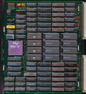
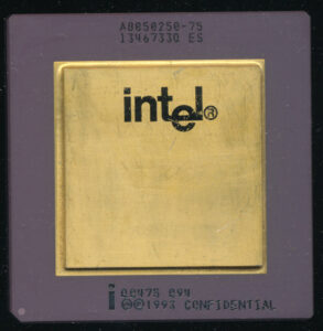
Navy 55910 ASSY 0125321 Controller A80386DX-25 (20MHz) Serial #2

The Control Board runs an Intel A80386DX processor.  On this particular board its a 25MHz chip, but note the crystal next to it is an 80MHz crystal.  A 386 internally divides the clock by 2, so the 80MHz clock is most like divided by 2 externally resulting in a 40MHz input to the 80386, and a 20MHz CPU clock.  I had another controller board with a 20MHz 80386 so they probably just used what ever they had available.  This is Serial # 2 afterall.  The 386 is supported by 4 27C256 EPROMs and 8 32K (CY7C198) SRAM chips, giving it 256K of SRAM.  In addition is 12 8k (CY7C185) 8K SRAM chips each with there own Pipeline Register.

A typical 386 system would have several MB of RAM, but this system is set up for real time data processing, as a DSP system, so the only data that needs to be in RAM is the control program itself, so 256K of system RAM is a great plenty.  Additional RAM is likely used solely for buffering data from the Hydrophones.

It would be interesting to know what this board was used for in more detail, but even if that never happens its an interesting board for its time.  Clearly a vast amount of effort went into designing and building the system.


Tags:
,

Posted in:
Boards and Systems

June 19th, 2021 ~ by admin

Intel P54CM Pentium: The Dual Pentium Processor

Intel Pentium P54CM – Q0475 Engineering Sample from November 1993

Today dual processors are incredibly common, even in home computing, and multicore processors even more common, but there was a time when this was not so.  There were of course multi-processor systems in the 80’s and early 90’s, but these required extensive additional hardware to support them.   Three main concerns for design multiprocessing systems are how to efficiently handle interrupts (which CPU handles what), how to ensure the caches are kept current (and not used if they aren’t), and how do processors share the same bus.

Bus sharing was largely handled already as busses have long been shared by all sorts of devices.  Interrupts were made easier by the release of the APIC (Advanced Programmable Interrupt Controller) standard by Intel in the early 1990’s.. The first version of this was implementing in the 82489DX IC.  Each CPU (486 or original P60/66) would need its own 82489DX (Local APIC) and then yet another one to work as an I/O APIC.  Clunky, but it worked.  The BIOS and OS were designed to help with cache coherency coupled with the a modified MESI protocols in the processors themselves for keeping track of what cache items were valid or not.

P54CM50-75 Q033 – Early October 1993 Sample – 75MHz modified Socket 5

After the release of the first (P5 Socket 4) Pentiums Intel decided to integrate  an APIC onto the CPU core itself.  This greatly simplified dual processor setups.  Within only a few months of the release of Socket 4, Intel was already working on the P54C Pentium.  These were to be on a whole new socket, Socket 5 (much to the annoyance to those who had just dropped some serious coin on a Socket 4 system).  The Socket 5 systems, using the Intel Neptune 430NX chipset, would support dual processor systems.  To do this Intel designed a separate Pentium Processor core called the P54CM, and originally, a separate, slightly modified socket for it.  The secondary socket had a slightly different pin out, and was to run the P54CM processor, OR, could be used as an OverDrive socket, with the Overdrive becoming a second CPU (why both, no one is entirely sure).

P54CM50-75 Q033 – Mod Socket 5 – Oct 1993 Q0475 Nov 1993 – Standard Socket 5

Samples of the P54CM debuted in October of 1993 using the new pinout.  Samples from just weeks later had reverted to the standard Socket 5 pinout, clearly someone at Intel decided that yet another socket (and package) design would be uneconomical.  The separate core, however, remained.

Early Pentium Print Ad shows the modified Socket.

The P54CM core was only produced in a very few specs, SX874 B1 stepping in STD Voltage (3.135V–3.465V) and the SX942 (STD) SX943 (VRE 3.3V–3.465V)  and SX944 (MD: faster timings on several pins/3.135V–3.465V) series in the B3 stepping.  There were also several ES versions made: Q033 P54CM50-75, Q0475, Q0519 and Q0520 with the B0 stepping and Q0543 with the B1 stepping.  These processors, including the production versions, were incredibly rare.  Very few companies used them in actual machines.  Why? Because a normal (providing it supported dual processing) P55C could be ran just as well.  The only real difference in the P54CM core was the DPEN/ output pin was driven low on RESET.  On a P54CM this pin is an output that tells the primary processor ‘hey a second processor exists’ while on the standard P54C, DPEN/ is an input.

SX874 – P54CM-B1 (with the FDIV bug) from October 1994

It turns out that the P54C/CM core ALSO has a CPUTYPE pin that can be be set to tell a system that the processor is a secondary processor or a primary (and early Pentium Dual boards had a jumper to do just this.)  You didn’t actually NEED a P54CM as the secondary processor. a normal P54C would work just fine.  There was even some trickery to allow a system to boot off of a secondary P54CM CPU, not officially supported by Intel, but in systems designed for redundancy, the DPEN/ pin could be overridden and the P54CM used to boot a system (normally the primary CPU would handle all the boot up duties and only enable the secondary CPU once it was ready).

Later Socket 5/7 Pentiums (C0 and later steppings) supported multiprocessing natively with a few exceptions.  The SU114/SL25H Pentium 200s did not have a functional APIC so thus were not DP compatible.  These were even mismarked by Intel, with the marking ‘VSS’ on the back.  That last ‘S’ means they were tested to support UP, DP and MP configurations, when in fact they were not, the code on the back should have been VSU (‘U’ means they were tested for MP, and uniprocessor, but NOT DP, as DP required a working APIC).  The SY045 (200) and SY037 (166) were also ‘VSU’ processors, not tested for DP use, likely because of some issue with the APIC.

Mismarked SU114 (VSS) and correctly marked SY045 VSU

Intel Overdrive processors suffer a similar fate, they will not run in the primary socket of a DP system, but will in the secondary socket.  This is mostly likely because the DPEN/ is not supported as an input on the Overdrive, so it wouldn’t know a secondary processor exists, a shame really as a dual OverDrive system would be pretty neat.

At he beginning of the P5 era Intel seemed to be all in on DP systems, but with the coming release of the Pentium Pro, they began to use Dual Processing as a way to differentiate their products.  DP support was removed in the next Pentium chipset (the FX Triton) only to later return in the HX Triton II.  The VX and TX Pentium Chipsets also lacked DP support.

Quite famously later in the 1990s Intel marketed the Pentium II/III with multi-processor support, and sold the Celeron as uniprocessor only.  It turned out that the lowly Celeron was quite happy to run in DP configuration, much to the annoyance of Intel, but joy of enthusiasts around the world.  Perhaps someone will figure out a way to run Pentium Overdrives in dual processor systems, if there is a will there tends to eventually be a way.


Posted in:
CPU of the Day