Archive for March, 2018

March 24th, 2018 ~ by admin

Making MultiCore: A Slice of Sandy

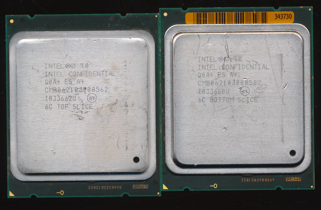
Intel Sandy Bridge-EP 8-core dies with 6 cores enabled. Note the TOP and BOTTOM markings (click image for large version)

Recently a pair of interesting Intel Engineering Samples came to The CPU Shack.  They are in a LGA2011 package and dated week 33 of 2010.  The part number is CM8062103008562 which makes them some rather early Sandy Bridge-EP samples.  The original Sandy Bridge was demo’d in 2009 and released in early 2011.  So Intel was making the next version, even before the original made it to market.  The ‘EP’ was finally released in late 2011, over a year after these samples were made.  Sandy Bridge-EP brought some enhancements to the architecture, including support for 8-core processors (doubling the original 4).  The layout was also rather different, with the cores and peripherals laid out such that a bi-direction communications ring could handle all inter-chip communication.

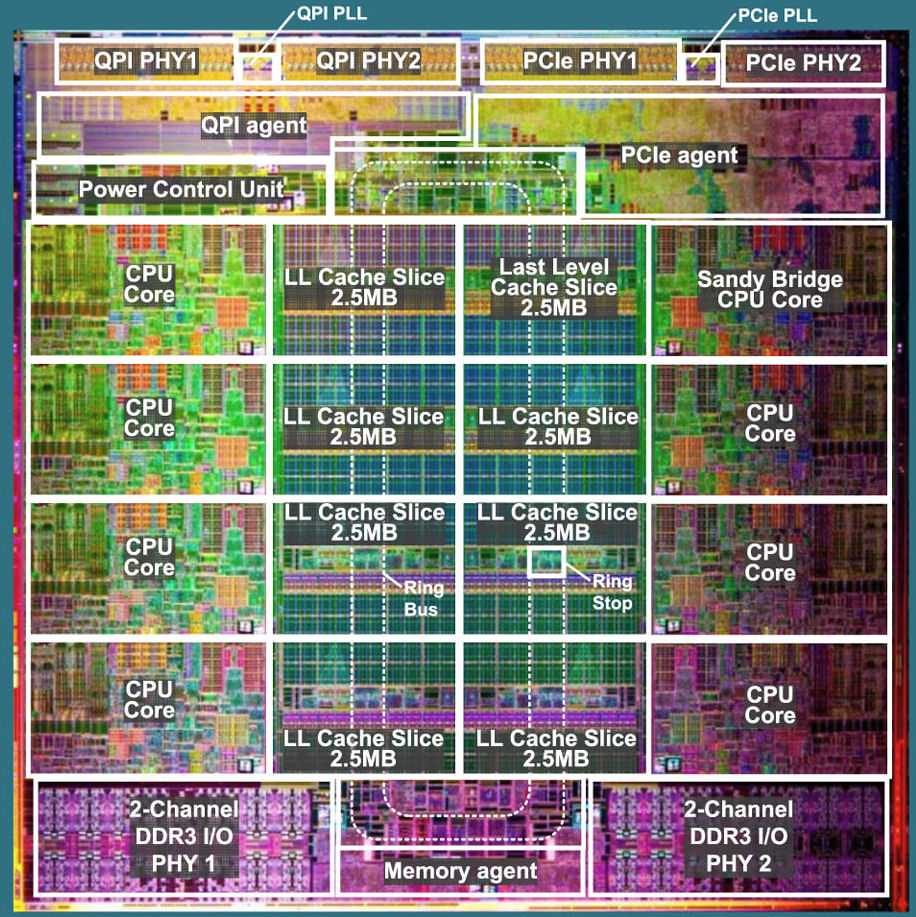
Sandy Bridge-EP 8-core die layout. Note the ring around the inside that provides communications between the peripherals on the top and bottom, and the 8-cores. (image originally from pc.watch.impress.co.jp)

Sandy Bridge EP supports 2, 4, 6 and 8 cores but Intel only produced two die versions, one with 4 cores, and one with 8 cores.  A die with 4 cores could be made to work as a dual core or quad, and an 8-core die could conceivably be used to handle any of the core counts.  This greatly simplifies manufacturing.  The less physical versions of a wafer you are making, the better optimized the process can be made.  If a bug or errata is found only 2 mask-sets need updated, rather then one for every core count/cache combination.  This however presents an interesting question..What happens when you disable cores?

That is the purpose of the above samples, testing the effects of disabling a pair of cores on an 8-core die.  Both of the samples are a 6-core processor, but with 2 different cores disabled in each.  One has the ‘TOP’ six cores active, and the other the ‘BOTTOM’ six cores are active.  This may seem redundant but here the physical position of the cores really matters.  With 2 cores disabled this changes the timing in the ring bus around the die, and this may effect performance, so had to be tested.  Timing may have been changed slightly to account for the differences, and it may have been found that disabling 2 on the bottom resulted in different timings then disabling the 2 on the top.

Ideally Intel wants to have the ability to disable ANY combination of cores/cache on the die.  If a core or cache segment is defective, it should not result in the entire die being wasted, so a lot of testing was done to determine how to make the design as adaptable as possible.  Its rare we get to see a part from this testng, but we all get to enjoy its results.

March 21st, 2018 ~ by admin

Intel’s Chipped Chips

Early Intel 8080A processor (no date code) chipped and used in a Uni kit

Typically when collecting something, be it coins, cars or CPU’s having the most pristine unblemished example is highly desirable.  However, sometimes, the best example is one that isn’t perfect, in coin collecting it may be a rare double struck coin, or some other flaw that actually makes the coin more valuable.

In the 1970’s Intel put together many development kits for it’s processors.  These were to help engineers, companies, and even students learn how to use Intel’s products. Intel made several kits specifically for University use, including one based around the MCS-80 processor and another around the MCS-48 microcomputer.  The 8080 University kit came with an 8080 processor, and a variety of support chips, including RAM, EPROMs (usually 1702s), clock drivers, bus drivers etc.  They were often a mix of packages, including plastic, and ceramic, with many chips being marked ‘CS‘ which is Intel’s designation for a Customer Sample.

Military MC8080A CS from a Uni kit. Multiple chipped corners. Such damage often was a result of improper packing in an IC shipping tube.

The price of the kits was kept low, the purpose was to get people use to using Intel products, not to make money.  Due to this, Intel tried to build the kits in the most efficient way possible.  Almost every 8080 University kit included a working, but cosmetically damaged C8080A processor.  These were typically the white/gold ceramic variety with a chipped corner.   It was very common to see a MC8080A or MC8080A/B military spec processor in a University kit, the processor would function fine, but had  some damage, enough that it could not be sold as a mil-spec processor (which has requirements for screening out such damage). The damaged chip would simply be tested, stamped ‘CS‘ and stuck in a kit, ths saving Intel money and keeping a working processor from being wasted.   The same thing happened with the MCS-48 University kits, these included chips such as the D8035 or C8748 MCU, and again, often shipped with damaged chips.

It turns out that the most correct, authentic chip, in a University Kit, was the cosmetically challenged, and in a way, this makes them more uncommon and more interesting.  Its due to their damage that they were selected for the special use in a University kit.  The irony is that many times it was the highest end military screened chips, that ended up getting used in one of the lowest end products.

March 15th, 2018 ~ by admin

CPU of the Day: Intel Jayhawk – The Bird that Never Was

Intel Jayhawk Thermal Sample – 80548KZ000000 QBGC TV ES – Made in April 2004 Just 3 weeks before it was canceled

Perhaps fittingly the Jayhawk is not a bird, but rather a term used for guerilla fighters in Kansas during the American Civil War.   It is also the name of a small town in California 150 miles Northeast of Intel’s headquarters in Santa Clara.  It was also the chosen code name for a Processor Intel was working on back in 2003.  In 2003 Intel was working on the Pentium 4 Prescott processor, to be released in 2004 and its Xeon sibling, the Nocona (and related Irwindale),  The Prescott was a 31 stage design made on a 90nm process.  There was hopes it would hit 4+ GHz but in production it never did, though overclockers, with the help of LN2 cooling were able to achieve around 8GHz.  Increasing the length of the pipeline helps allow higher clock speeds, the Northwood core had a 20-stage pipeline so the Prescott was a rather big change.  There is a cost of lengthening the pipe, processors don’t always execute instructions in order, often guessing what will come next to speed up execution.  This is called speculative execution, processors also guess what data is to be needed next, and stick it in cache.  If either of these ‘guesses’ is wrong, the processor needs to flush the pipeline and start over, at a comparatively massive hit in performance.  This is what performance doesn’t always scale very linearly with clock speed.

Intel figured that this wouldn’t be an issue and so the Prescotts successor was to have a 40-50 stage pipeline.   THe hopes were for 5GHz at 90nm and 10GHz at 65nm. The desktop version was known as Tejas, and the server version, Jayhawk.  Initially these were to be made on the 90nm process, same as Prescott, before being transitioned to a 65nm process.  It increased the L1 cache to 24k (some sources say 32k) from the Prescotts 16k.  The Instruction trace cache was still 16k micro-ops, though this could have been increased.  L2 cache would have been 1MB at introduction and 2MB once the processor moved to a 65nm process.  Eight new instructions were to be added called ‘Tejas New Instructions’ or TNI, these later would become part of the SSSE3 instructions released with the Core 2 processor.  It also would bring ‘Azalia’ Intel’s High definition audio codec, DDR2 support, a 1066MHz bus, and PCI-Express support.  It turns out there was a problem….

Read More »