Archive for October, 2014

October 30th, 2014 ~ by admin

SGS-Ates M380 and GI LP8000 – 8 Bits for Europe

SGS-Ates M380B1 - 1977

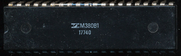
SGS-Ates M380B1 – 1977

In the 1970’s the computer age was booming.  New processor designs were being pushed out by the month, and computers to use them were being designed and outdated just as fast.  Not all markets were growing as fast as the American market, or could support the newest, most complex, and expensive designs.  Thus, it was common for semiconductor companies to design chips specifically for these markets.  Europe was considered one of these markets, where simpler more affordable devices were easier to sell, thus CPUs were made specifically for the European market.  Many of these designs are still nearly impossible to find outside of Europe.

General Instruments was one such company.  Their premier processor, the CP1600, was a 16-bit deign based on the PDP-11.  It was one of the first NMOS 16-bit processors (along with the TI9900) and was released in 1975.  GI also had the PIC line of 8-bit MCUs for control oriented tasks, which is still in production today.  GI wanted a design for the European market so in 1976 released the LP8000, LP for Logic Processor.  The LP8000 was a 3-chip simple processor and cost a mere $10.  It could execute 48 instructions (including ADD, but subtraction was not supported directly) at a clock speed of 800 kHz and was made on a PMOS process. The chipset consisted of the LP8000 processor which contained the ALU and 48 8-bit registers as well as the accumulator a 6-bit address bus and 8-bit of I/O.  Combining the 6-bit address and 8-bit I/O busses allowed the LP8000 to directly address 16K of memory.  The 11-bit Program Counter was contained off chip, on the LP6000 which also contained an additional 16 lines of I/O and 1K of ROM for program storage.  Clock generation was provided by the LP1030 and memory expansion was handled by the LP1000 (which also includes a 11-bit PC for interfacing up to 2K of memory) while the LP1010 handled I/O expansion.  In order to be successful in Europe GI needed to find a European partner who could make, market and sell the design.
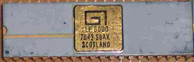
GI LP8000

GI LP8000

That partner ended up being SGS-Ates of Italy (which later would become ST Microelectronics).  SGS-Ates second sourced the LP8000 as the M38 (or M380) series.  The M380 was the processor element, while the M382 was the 1K ROM equivalent of the LP6000.  In addition SGS-Ates made the M381 which had 18 bytes of RAM and 768 bytes of ROM as well as the PC.  Like the LP8000 the M380 drew about 1 Watt of power and required a +5V and -12V supply (or a -5V and -17V).  The M380 was rather short lived as SGS-Ates soon licensed the Zilog Z80 which was a much more powerful, yet still inexpensive, design.  When SGS-Ates purchased Mostek from United Technologies they added yet another 8-bit design, the F8, which Mostek had licensed from Fairchild.  These processors quickly replaced the M380/LP8000 and with no market, it faded into obscurity.

Posted in:
CPU of the Day

October 15th, 2014 ~ by admin

Has the FDIV bug met its match? Enter the Intel FSIN bug

Intel A80501-60 SX753 - Early 1993 containing the FDIV bug

Intel A80501-60 SX753 – Early 1993 containing the FDIV bug

In 1994 Intel had a bit of an issue.  The newly released Pentium processor, replacement for the now 5 year old i486 had a bit of a problem, it couldn’t properly compute floating point division in some cases.  The FDIV instructions on the Pentium used a lookup table (Programmable Logic Array) to speed calculation.  This PLA had 1066 entries, which were mostly correct except 5 out of the 1066 did not get written to the PLA due to a programming error, so any calculation that hit one of those 5 cells, would result in an erroneous result.  A fairly significant error but not at all uncommon, bugs in processors are fairly common.  They are found, documented as errata, and if serious enough, and practical, fixed in the next silicon revision.

What made the FDIV infamous was, in the terms of the 21st century, it went viral.  The media, who really had little understanding of such things, caught wind and reported it as if it was the end of computing.  Intel was forced to enact a lifetime replacement program for effected chips.  Now the FDIV bug is the stuff of computer history, a lesson in bad PR more then bad silicon.

Current Intel processors also suffer from bad math, though in this case its the FSIN (and FCOS) instructions.  these instructions calculate the sine of float point numbers.  The big problem here is Intel’s documentation says the instruction is nearly perfect over a VERY wide range of inputs.  It turns out, according to extensive research by Bruce Dawson, of Google, to be very inaccurate, and not just for a limited set of inputs.

Interestingly the root of the cause is another look-up table, in this case the hard coded value of pi, which Intel, for whatever reason, limited to just 66-bits. a value much too inaccurate for an 80-bit FPU.

October 11th, 2014 ~ by admin

Why the Zilog Z-80’s data pins are scrambled

Zilog Z80A CPU -1978

Zilog Z80A CPU -1978

Ken Shirriff has an excellent write up about the Zilog Z80 and why its pin-out, specifically the Data lines, is a bit convoluted.  Rather then being in order (such as D0-D7) the original Z80 is D4,D3.D5,D6,D2,D7,D0,D.  Its functional but its not pretty and can lead to some interesting PCB layout issues.  Ken uses data/imaging from the Visual6502 project to look at the on die reasons for this.  Essentially it came down to saving die space. there literally was not enough room to route the data connections within the confines of the die size.  Keeping the die size small allowed Zilog, and its many second sources), to keep prices down.  In the early days Zilog contracted Mostek to make much of their processors, so die size and the associated cost were a big issue.

Tags:

Posted in:
Research