January 20th, 2014 ~ by admin
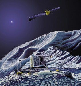
Rosetta Comet Chaser – Dynex 1750
The ESA’s comet chaser Rosetta has just today awoken from a long deep sleep on its comet chasing (and landing) mission. The solar powered spacecraft was launched back in 2004. It is based on the Mars Mariner II (itself based on the Voyager and Galileo) spacecraft design of the early 1990s (when the mission was first conceived.) Main differences include using very large solar arrays versus a RT (Radioisotope Thermal Generator) and upgraded electronics.
In order to conserve power on its outward loop (near Jupiter’s orbit) most all systems were put to sleep in June of 2011 and a task set on the main computer to waken the spacecraft 2.5 years later and call home. The computer in charge of that is powered by a Dynex MAS31750 16-bit processor running at 25MHz, based on the MIL-STD-1750A architecture.
A reader recently asked why such an old CPU design is still being used rather then say an x86 processor. As mentioned above the Rosetta design was began in the 1990’s, the 1750A was THE standard high reliability processor at the time, so it wasn’t as out of date as it is now that its been flying through space for 10 years (and 10 years in the clean room). The 1750A is also an open architecture, no licenses are or were required to develop a processor to support it (unlike x86). Modern designs do use more modern processors such as PowerPC based CPUs like the RAD750 and its older cousin the RAD6000. Space system electronics will always lag current tech due to the very long lead times in their design (it may be 10 years of design n the ground before it flies, and the main computer is selected early on). x86 is used in systems with 1) lots of power, and 2) somewhat easily accessible. Notably the International Space Station and Hubble. x86 was not designed with high reliability and radiation tolerance in mind, meaning other methods (hardware/software) have to be used to ensure it works in space.
Currently the ESA designs with an open-source processor known as the LEON, which is SPARC-V8 based.
January 17th, 2014 ~ by admin
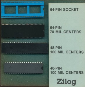
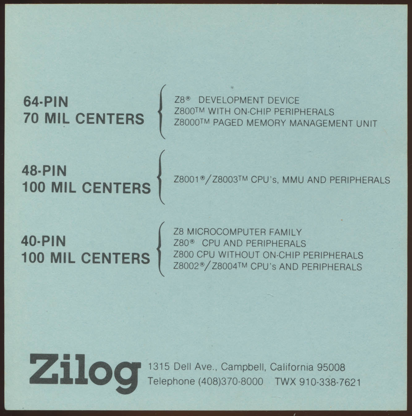
Zilog Packages available in 1985
Last week we showed you an educational kit from Zilog showing the process involved in making and assembling a Z80 processor, from polished wafer to packaging. Zilog also made a kit for marketing the various packages used. This kit contains a shrink DIP 64 pin socket, a shrink DIP 64pin package, a 48 pin DIP and 40 pin DIP, all the common packages used at the time.
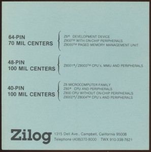
Zilog Packages – Z8 Z80 Z800 and Z8000
At the time is a little hard to track down as no date is provided with this kit. We can get very close though looking at the back where Zilog lists which devices are available in these packages. The usual Z80 and Z8000 series are both there as well as the Z8 microcontroller family. The one odd-ball is the Zilog Z800. The Z800 was an upgraded Z80 released in 1985, adding on chip cache an MMU and a vastly expanded instruction set (over 2000 instruction/addressing modes). It was wholly unsuccessful partly do to bad marketing by Zilog, and partly because it did more then it needed to. It never entered mass production, and by 1986 Zilog has redesigned it, converted the design to CMOS (from NMOS) and released it as the Z280 which met the same fate as the Z800. It seemed that making an overly complicated Z80 wasn’t what the market wanted. THe Z180 (designed by Hitachi) and the Zilog eZ80 (released in 2001), have enjoyed much wider success, mainly because they kept closer to the simplicity of the original Z80.
So when was this kit put together? Likely 1985, as the Z800 was nly talked about for a few months before quietly being put away.
January 9th, 2014 ~ by admin
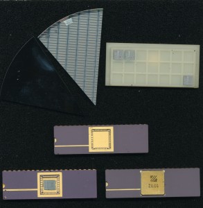
Zilog Z-80 Kit – Click for full size
Here is a neat kit from Zilog. Its an Educational Kit showing some of the steps of producing a Z-80 processor. It includes:
- A raw polished wafer slice before any etching has occured. This is what a processor starts out with (sliced from a single large ingot)
- A slice of an etched wafer. In this case it appears to be some sort of memory, but the process is the same for a processor.
- Several cut die, these are cut from a wafer after testing. The red dot notes that these particular dice failed one or more of the tested and should be discard. Thats probably why they made it into this kit rather then a saleable device.
- An bare unfinished package. These packages are rarely if ever made by the company making the processor. They are made by companies such as NGK (who also makes spark plugs) and Kyocera. The bottom of the die cavity is usually connected to the ground pin of the package.
- Next is a package with the die placed in the die cavity. No bonding wires are installed in this example but that would be the next step. The very fine gold bonding wires connect the pad ring on the edge of the die, to the pads in the die cavity. Those [ads are connected through the package to the 40 pins of the ceramic DIP package.
- Finally we have a completed device. The lid is usually soldered or brazed onto the package and markings applied. The marking on this example make it a ‘Marketing Sample’ as they are there solely for looks, rather then to identify the device, its date, and lot.
These types of kits were produced for educational use, and given to schools, as well as sales people to assist in marketing Zilog’s various products
January 6th, 2014 ~ by admin
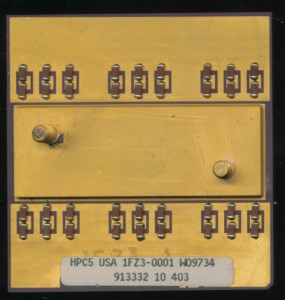
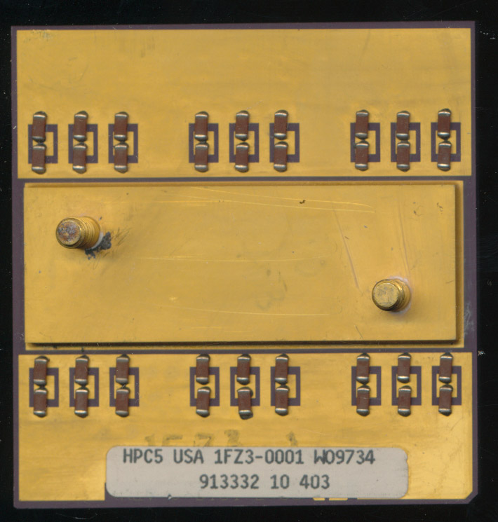
HP 1FZ3-0001 PA7000 66MHz – 1991
Welcome to 2014 and a new year of exciting processors and technology finds at the CPU Shack Museum. We’ll spend the next couple weeks posting some of the more interesting finds of 2013 that didn’t get posted before.
The PA-RISC was HP’s architecture meant to unify all their non x86 processors of the 1980’s. The project began in the 1980’s and produced over a dozen processors designs, ending with the PA-8900 in 2005, though the Itanium borrows heavily from the PA-RISC line. HP discontinued support for PA-RISC servers in 2013 and recently announced that they will discontinue use of the Itanium as well.
Early PA-RISC processors were multi-chip designs such as this PA-7000. The PA-7000 pictured is only the CPU, the FPU was a separate chips, as was the L1 caches (no support for L2 caches). A memory controller was also a separate chip. Made on a 1 micron process the PA-7000 had 580,000 transistors and ran at 66MHz. Early versions had 2 lugs for the heatsink on the package while later versions had only a single lug.