
First & Last AMD Socket A Athlons – Thunderbird vs. Barton – Part 1
Introduction
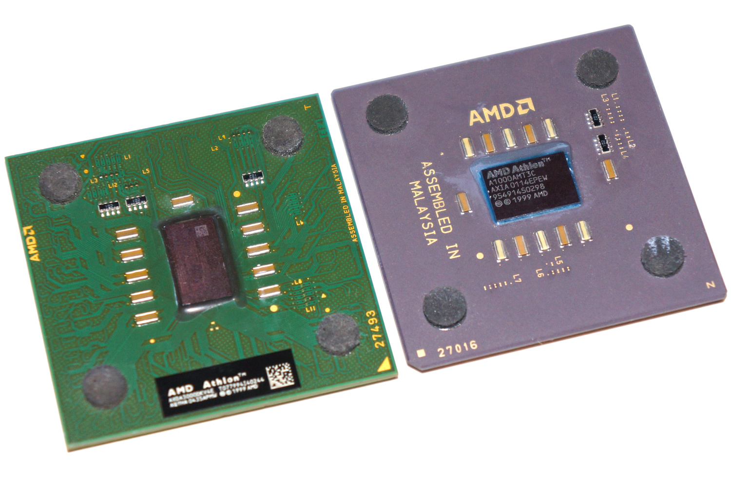
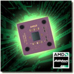 The AMD Socket 462 or Socket A, was a rather interesting and long-lasting CPU Socket. The first models of Socket 462 processors appeared in the summer of 2000, they were just the first representatives of the AMD Athlon “Thunderbird” in a ceramic case with a clock frequency of 600 MHz, and with 256 KB of L2 cache , an effective system bus frequency of 200 MHz, with MMX support instructions and their own 3DNow !, of course, there was no question of any SSE in those days. Produced ” Thunderbirds” at 180 nm. tech process, the operating voltage was set in the range of 1.70-1.75 volts, and the maximum heat dissipation was 72 watts for the older model 1400 MHz versions. These replaced the old Slot A cartridge based Thunderbirds, made possible by the L2 cache being moved on die instead of off die (in similar fashion to Intel’s Coppermine Pentium IIIs moving to S370 from Slot 1).
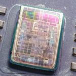
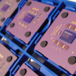
Thunderbird die exposed
The last representative that was designed for Socket 462 was AMD Athlon XP+ using the “Barton” core, released in early 2003, which retained its position throughout 2004. With “Barton” the ceramic case is a thing of the past, being replaced by a Organic PGA package. The process has decreased to 130 nm, the L2 cache capacity has doubled, the system bus frequency has doubled, and the clock speeds have exceeded 2.2 GHz.
The fastest model had a real frequency of 2200 MHz and a performance rating of 3200+, the operating voltage was 1.65 V, and the TDP was 77 W with a 400FSB. These was also another AXDA3200 with a 333 FSB, this actually clocked slightly faster as 2.333GHz, but was given the same PR rating due to its slightly slower FSB. The processor acquired the first generation SSE instructions, and the motherboards created for it in that day now added support for dual-channel operation of the RAM. If we add here that the first motherboards based on Socket 462 worked with SDRAM memory, and the subsequent ones with DDR-SDRAM, then according to a number of indicators there is a twofold increase in the main characteristics of the platform within the framework of one socket.
Such a funny comparison reminded me of today, where from the time the first generation of AMD Ryzen processors appeared in 2017, until the last (fourth gen), which debuted at the very end of last year (2020), all processors also had one AM4 socket. Ryzen performance gains across all four generations are clearly exemplified by the following slides:
AMD hasn’t had much of a problem with processor support before, although AMD has officially announced that Ryzen 5000 series desktop will only be supported on boards with 400 and 500 series chipsets. Therefore,  on motherboards released for the first generation Ryzen, it will not work to use the latest generation processors in an official way. Although there is information on the network that there are cases of using Ryzen 5000 series processors on motherboards with the older X370 chipset, but the official position of AMD has already been announced above.
In the wake of such analogies, I thought, why not compare the first and the last Athlons for Socket 462 on several motherboards at the same clock frequency, with the same system configuration? You will find out the result of what came out of this by reading this article to the end.
Continuation of the Idea
 The essence of the idea is simple – take the first AMD Athlon based on the “Thunderbird” core with a 200 and 266 MHz system bus and a clock speed of 1 GHz and an AMD Athlon XP representative on the “Barton” core with a similar round frequency of one GHz, and compare them with each other to find out how much the first generation loses to the last one. During the existence of Socket 462, several generations of processors with different cores have changed on it: Thunderbird – Palomino – Thoroughbred – Thorton – Barton. This will be an interesting test of raw architecture improvements of the core. all other things being as equal as they can be.
 A head-on comparison alone will not be enough, since the winner is known in advance, the only interesting thing is the total win and loss percentage relative to each other, so I decided to add the chipset component to the comparison. The continuation of the idea was to take motherboards on the first and last chipsets produced for a given socket to see how each CPU architecture would respond. And for more interest, I decided to add intermediate chipsets for Socket 462 to the comparison, so that you can already see the dynamics of performance growth from chipset to chipset, and all this with unchanged characteristics of all combinations of tested platforms.
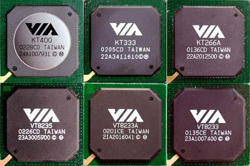
Let me remind you what chipsets were produced for the Socket 462 platform over the entire period of its existence. The first was the VIA Apollo KT133 chipset, which was released by the Taiwanese VIA Technologies in 2000. The chipset supported Athlon and Duron processors with a system bus frequency of 100 MHz (effective EV6 bus frequency was 200 MHz), and used PC100 and PC133 SDRAM-memory in synchronous and asynchronous modes. Subsequently, VIA Technologies engineers released an updated version of the chipset, adding the letter “A” at the end, so the chipset turned out – KT133A, which already had official support for the 133 (266) MHz bus. This tradition of “finishing” chipsets became the norm, and subsequent chipsets were initially released as they are, and then an improved version with the “A” suffix was released.
AMD debuted Socket A Athlons with a shipset of its own, This was the AMD 750/751 Irongate in 1999. It could use AMD 756 South Bridge, or more commonly, the VIA 686A. Initial versions were buggy (having issues with AGP 2X support) but this was later worked out. AMD made their own chipsets mainly as a hedge, to ensure the platform had support in case VIA or one of the other chipset manufacturers had issues making one.
KT133 was followed by KT266, which acquired support for new Athlon XP processors and, accordingly, old Athlon, Duron, and at the same time Sempron (the new name for the Duron). The main feature of the new chipset was the new high-speed DDR-SDRAM standard PC2100 RAM as well as support for 4GB of RAM (up from 1-1.5GB) It was the first mainstream chipset to support next-generation memory. At that time Intel supported expensive and not very efficient RIMM memory made by RAMBUS (mainstream i845 motherboards used SDRAM). The KT266 also introduced V-link, a special dedicated bus linking he North and South Bridges, replacing what was once handled by the PCI bus, allowing for much more bandwidth.
AMD released the 761 chipset with 4GB of DDR support in late 2000 (and for some time it was the fastest). Backed again by either the VIA’s 686B or AMD’s 766 Southbridge. In 2001 AMD released the 762, which supported dual processors (AMD Athlon MPs) as well as DDR and AGP 4X like the 761. This proved a popular chipset for dual systems as other chipsets did not support SMP. The South Bridge was later revised to add hardware RNG (the 768 south bridge, but early versions had defective USB support, requiring the use of a separate PCI USB card). One limiting factor of the AMD Chipsets is they still used the PCI bus to link to the South Bridge, though in practice, this wasn’t a great limit for most things.
When the faster DDR-SDRAM of the PC2700 standard, operating at 333 MHz, appeared, a corresponding chipset was needed, which became the VIA KT333. This is also the last chipset that can work with AGP 2x video cards, but it can also work in AGP x4 mode =) In fact, KT333 is a logical continuation of KT266A, which did not differ much from it, so after the release of KT333 its improved version KT333A did not follow. The KT333 has proved quite popular as since it supports 3.3V AGP, it is the last, and fastest chipset to run 3Dfx video cards. Running a 333FSB 2.33GHz AXDA3200DKV4D Athlon on one of these boards, will beat a P4 3.06GHz NW on one of the few P4 chipsets to support 3.3V AGP, the SIS645DX.
 The next set of logic that appeared towards the end of 2002 was already noticeably different from all the previous ones. The new VIA KT400 chipset received an even faster V-Link bus and also brought support for AGP 8x video cards. The disk subsystem has also accelerated, thanks to the support of the UDMA133 data transfer protocol, as well as support for high-speed USB 2.0 ports. At the beginning of the next year, VIA improved this chipset as well, releasing a faster version of the VIA KT400A. Subsequently, motherboards based on this chipset could be equipped with a south bridge – VIA 8237, which provided support for a new data transfer interface – SATA. It is the 400 series that the main majority of motherboards for AMD Socket 462 processors will run on.
In mid-2003, VIA Technologies introduced the next chipset – KT600, designed for motherboards with AMD Athlon XP processors with 400 MHz FSB. There were only three differences from the KT400A:
1. The chipset’s memory controller acquired FastStream64 technology (using a block of prefetch buffers to reduce memory controller latencies) with support for single-channel DDR400 (PC3200) – a kind of response to Nvidia nForce2.
2. The VIA VT8237 south bridge was supplied with an integrated SATA / RAID controller with the ability to create disk arrays RAID 0 + 1 and JBOD.
3. “New” sound – VIA Vinyl Six-TRAC Audio, which was an old VT1616 codec with a new name VIA Vinyl Six-TRAC, connected via a standard AC’97 interface.
And that’s all.
In 2004 the last chipset from VIA – The KT880 was presented. The only significant difference that should have affected the speed characteristics was the presence of a dual-channel memory controller with support for DDR-SDRAM DDR400 (PC3200) memory. From the quantitative characteristics: the amount of supported memory has increased to 4 GB, a gigabit LAN module has appeared, the number of USB 2.0 ports has increased to eight. The chipset was released after the glory of all AMD Athlon XP and did not make much competition with the popular nForce2, although the performance gap from the Nvidia product was no longer as great as in the case of the KT600, but it was still there.
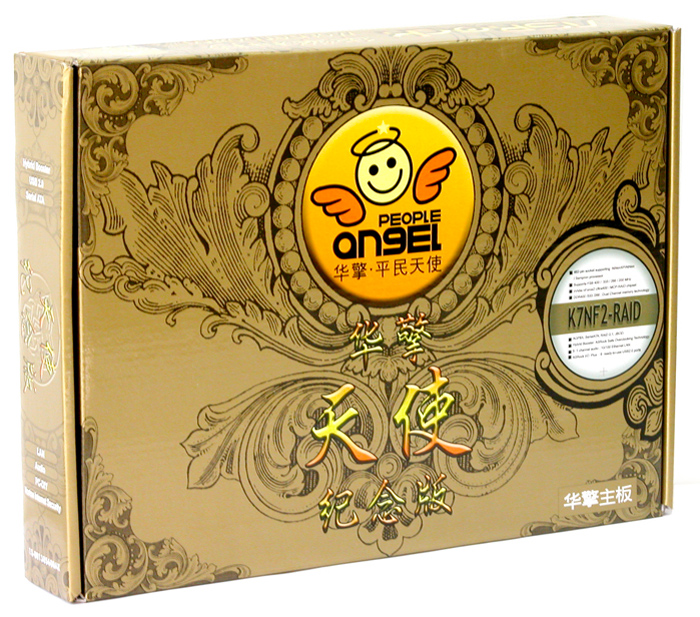
ASRock K7NF2-RAID “Commemorative Edition of Civilian Angel Collection
The first chipset from Nvidia was released at the end of summer 2002 under the name nForce2 and nForce2 Ultra (the Ultra prefix spoke about support for a 2-channel mode of the processor with RAM). A bit later, in May 2003, the updated NForce2 Ultra 400 chipset was released, which supported the system chipset at 400 MHz and a dual-channel memory controller with the same speed characteristics. Various variations of the south bridge could additionally give the user an audio system – SoundStorm with the ability to encode sound in Dolby Digital 5.1 format in real time, two Ethernet network adapters, Gigabit Ethernet, or native support for the Serial ATA interface. But the main benefit of Nforce chipsets was excellent and convenient overclocking potential and performance, which was higher than that of all competing parties. At that time, a common phrase was: “Do you have a motherboard based on Nforce or not?”, Which reflected the whole essence of choosing a motherboard based on Socket 462.
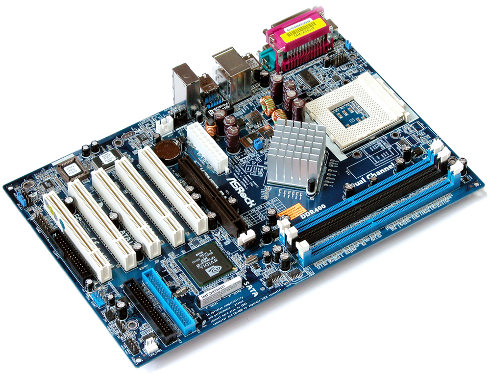
Released for the 3rd Anniversary of ASRock in 2005, perhaps the rarest nForce2 Ultra400 motherboard
Of course, the entire assortment is not limited to these chipsets, there were also SiS 7xx series, some with integrated graphics but none supported over 3GB of RAM and the Acer Labs M164x ALiMAGiK chipsets which were stuck at AGP 4X, 3GBs of RAM and DDR266 max, but I do not want to take into account the representatives of the Low-end sector, this applies to both processors and motherboards themselves with the corresponding chipsets.
Test participants
In this section, I will present those motherboards, processors and RAM that will participate in today’s testing.
Let’s start with the processors. AMD Athlon 1 GHz Thunderbird core will be represented by two models Athlon 1000B with FSB = 100 (200) MHz and x10 multiplier, and Athlon 1000C with FSB = 133 (266) MHz and x7.5 multiplier.
Athlon XP using the Barton core will be played by the only representative with a unlocked Athlon XP-M multiplier, which will also be set depending on the system bus frequency to either x7.5 or x10.
The settings for CPU-decoding instructions were set to maximum performance in BIOS.
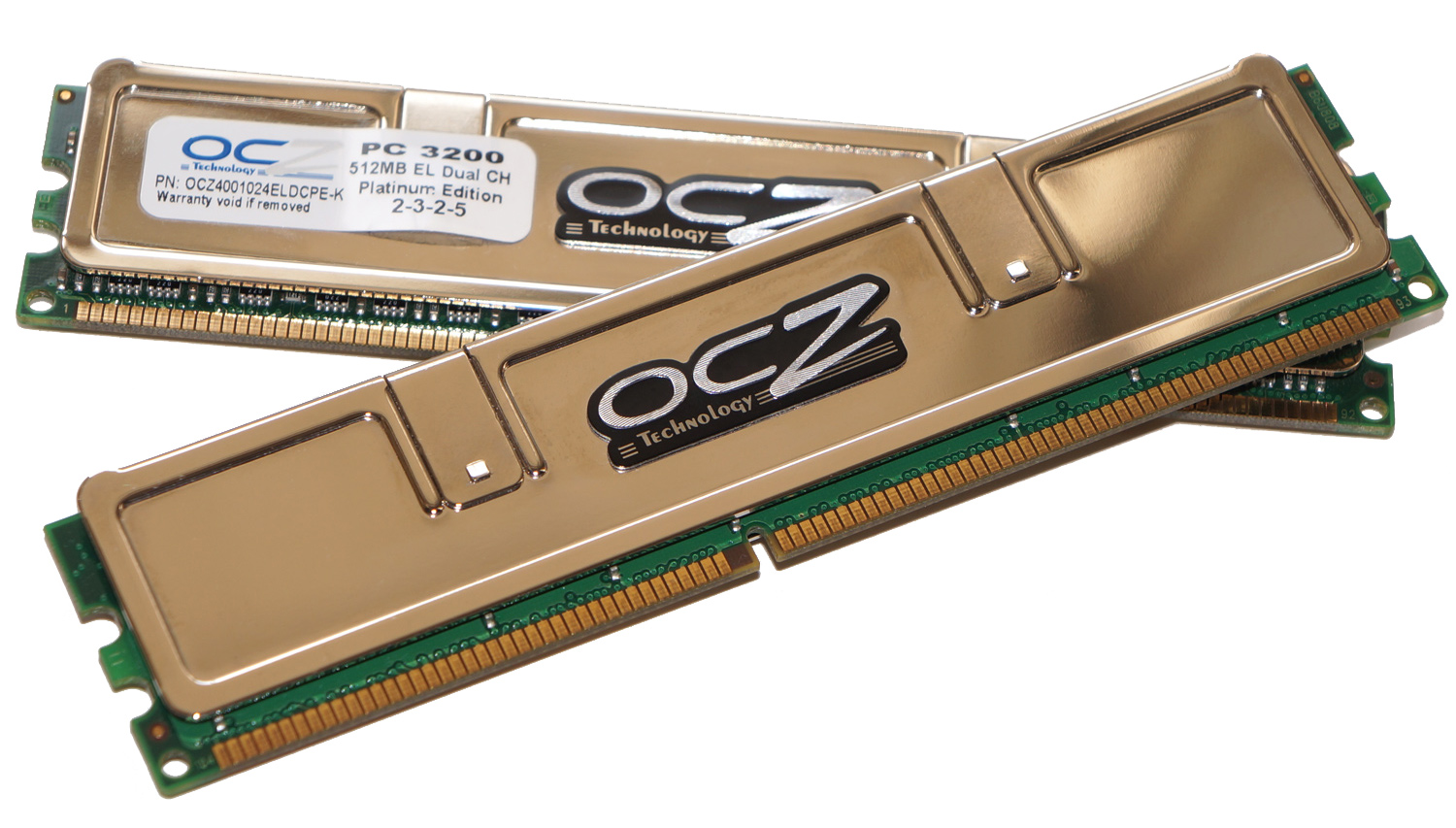
To minimize losses from the side of RAM, I chose a 512 MB x 2 KIT from OCZ – PC3200 EL Platinum Edition (OCZ4001024ELDCPE-K) with timings 2-3-2-5 will act as a DDR-SDRAM kit. These memory sticks are based on Winbond CH-5 chips, which will be enough for all frequencies, including 400 MHz. Memory timings for all platforms were set to the minimum values of 2-2-2-5 1T. Performance presets for sub-timings were similarly set in BIOS to FAST or ULTRA. Therefore, the results of the RAM subsystem also depend on the motherboard and its BIOS.
For SDRAM, the total memory capacity was 768 MB (256 MB + 512 MB) with the lowest possible timings that the motherboard allowed to install. In a word, all settings were reduced to the maximum performance of all systems.
For the final testing, I selected, or rather selected from the five motherboards I have. I did not take second-tier motherboards like ECS, Acorp or Gigabyte, but settled on the time-tested ASUS, ABIT and EPOX.
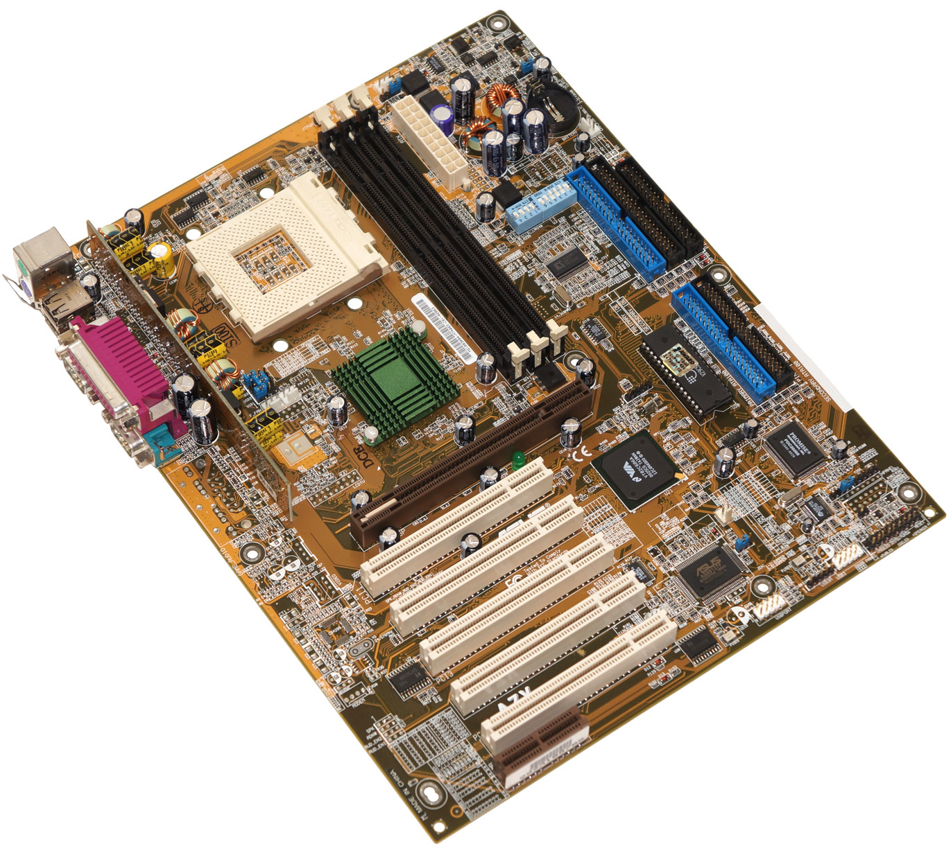
ASUS A7V – KT133
The very first motherboard will be ASUS A7V based on the VIA Apollo KT133 chipset, from which the history of AMD Athlon processors on Socket 462 began.
ASUS A7V – KT133 – With DIP Switches
From the photo you can see that the motherboard has a fairly large size, on which there are five PCI slots, one AGP Pro 4x (with Fast Writes support) and one AMR for an internal modem or sound card. There are two IDE controllers on the board, each of which can connect two hard drives. The first controller is a standard ATA-66, in the second case a controller from Promise PDC20265 is used, supporting the faster ATA-100 standard. The number of USB for its time is quite large – 7 ports.
For overclocking, it is possible to adjust the FSB frequency in the range from 90 to 146 MHz in 1 MHz steps. The processor supply voltages vary from 1.1 to 1.85 V, in 0.05 V steps. The multiplier can be changed from 5 to 12.5. Bus overclocking can be done through BIOS (JumperFree mode), or by means of Dip-switches on the motherboard itself. The processor multipliers can only be changed with the Dip switches on the board.
Riser mounted VRMs.
But, perhaps, the most distinctive feature of this board is the implementation of the VRM in the form of a removable module, which is located on a separate board and is installed perpendicular to the motherboard. Such a technical solution is quite rare, the pluses include the presence of free space around the socket, for the possibility of installing more overall cooling systems and the ease of repairing the VRM.
Although the FSB frequency range lies in the 90 to 146 MHz limit, the only and at the same time standard FSB frequency is 100 MHz. My efforts to overclock it only allowed us to overpower 118 MHz. This is a good result however for the KT133, at one time the reviewers of this board hardly crossed the 111 MHz threshold. Another feature of the board is the fact that the minimum TRAS timing can be set to 6, there is no option to select 5.
On the whole, the board made a good impression, it can be seen that ASUS approached the implementation of its first motherboard for AMD Athlon processors based on the “Thunderbird” core. But installing Barton into this board is not so simple. Initially, one of the first BIOS versions was flashed on the board, but after installing “Barton” in it, I still saw POST, but Windows could not be installed. When booting from an SSD with Windows XP already installed, the system worked extremely unstable, even the screenshots were saved “corrupted”. Having updated the version to the latest beta 1012.01a dated 09/13/2002, all the above problems disappeared and Windows XP was installed from scratch. But not every motherboard with the VIA KT133 system logic can support processors based on the «Barton» core, it depends primarily on the motherboard manufacturer and his attitude to the technical support of their products.
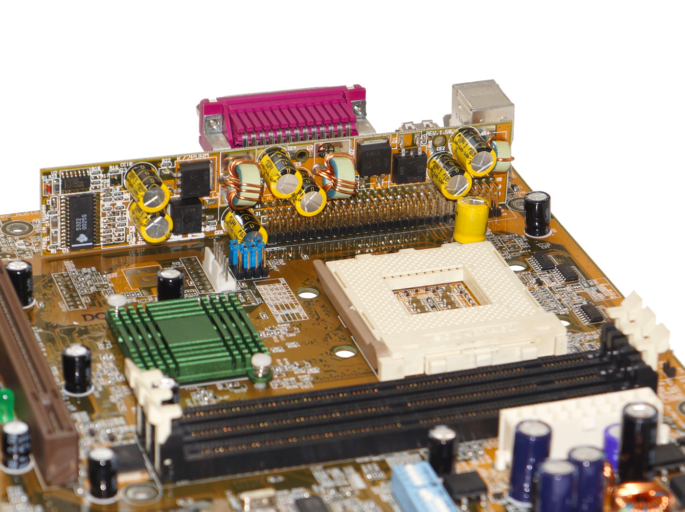
ABIT KR7A – KT266A
The honor of the VIA KT266A chipset will be protected by ABIT KR7A. This is, like the previous full-size motherboard, and even made directly in Taiwan. When you take it in your hands, you can see that this is not just an ordinary model.
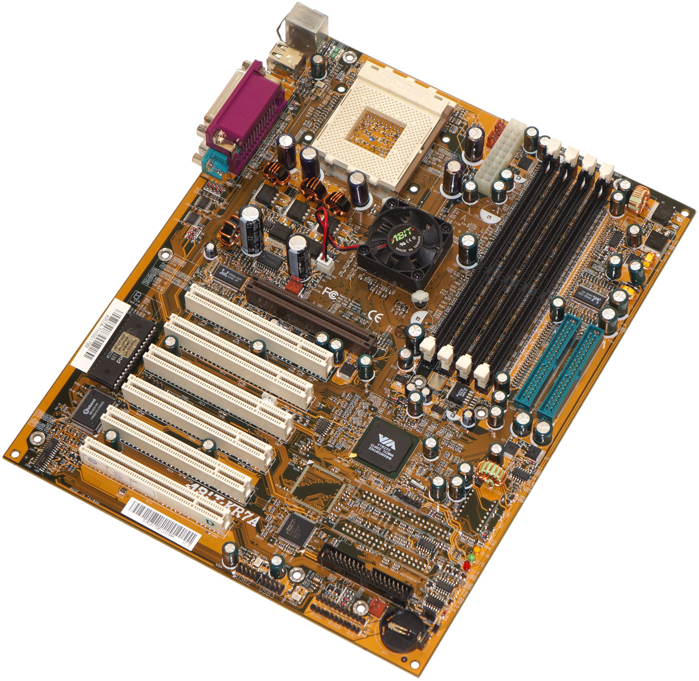
ABIT KR7A, VIA KT266A chipset
There are 6 PCI slots on the motherboard, the AGP 4X slot supports various video cards, including AGP 2x video cards powered by 3.3 V. The number of slots for RAM is four, which was also a rare occurrence for those times, you can install 3 GB of RAM, or 4 GB when using registered memory modules. Three-phase VRM boards are made up of powerful MOSFETS and sufficiently capacious filter capacitors, which makes it possible (via BIOS) to change the main voltages: Vcore, Vmem and Vio in a fairly wide range.
On the north bridge of the chipset, there is a heatsink with a fan without a speed sensor, which also blows a side stream to the board’s power supply regulators. As befits an overclocking board, it has three diagnostic LEDs that visually indicate the status of the board.
But all the most interesting goodies are concentrated in the BIOS, in the Softmenu III section, here ABIT engineers are, as always, at their best! The processor multiplier can be changed in the range from 5 to 13 and higher in 0.5 steps, the FSB frequency changes from 100 to 200 MHz in 1 MHz steps, all possible voltages are changed: Vcore, Vmem, Vio, Vagp in a wide range, there is a choice of timings for RAM including TRAS = 5. There is also a choice of a divider for FSB and other buses in a ratio of 3:2:1 and 4:2:1, as well as an important parameter Fast CPU Command Decode, which in Ultra mode gives a noticeable performance boost. This board is designed for overclocking and easily overcomes FSB frequencies> 160 MHz, and some overclockers have passed tests at FSB frequencies of 200 MHz and higher, up to 215 MHz.
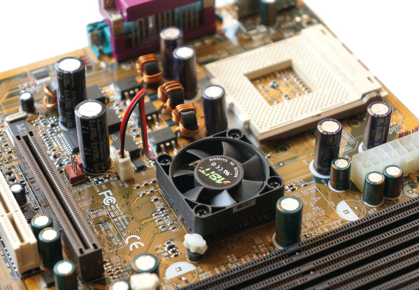
EPOX EP-8K3A – KT333
Moving on to KT333. The test motherboard will be a model from EPOX – EP-8K3A. The motherboard has 6 PCI slots, AGP x4 port, with the ability to support both 1.5V and 3.3V video cards, three DIMM slots with support for up to 3 GB of RAM. A three-phase VRM with 12 capacitors is sufficient for good overclocking, which depends entirely on the BIOS of the motherboard, the fashion for jumpers and switches has already gone.
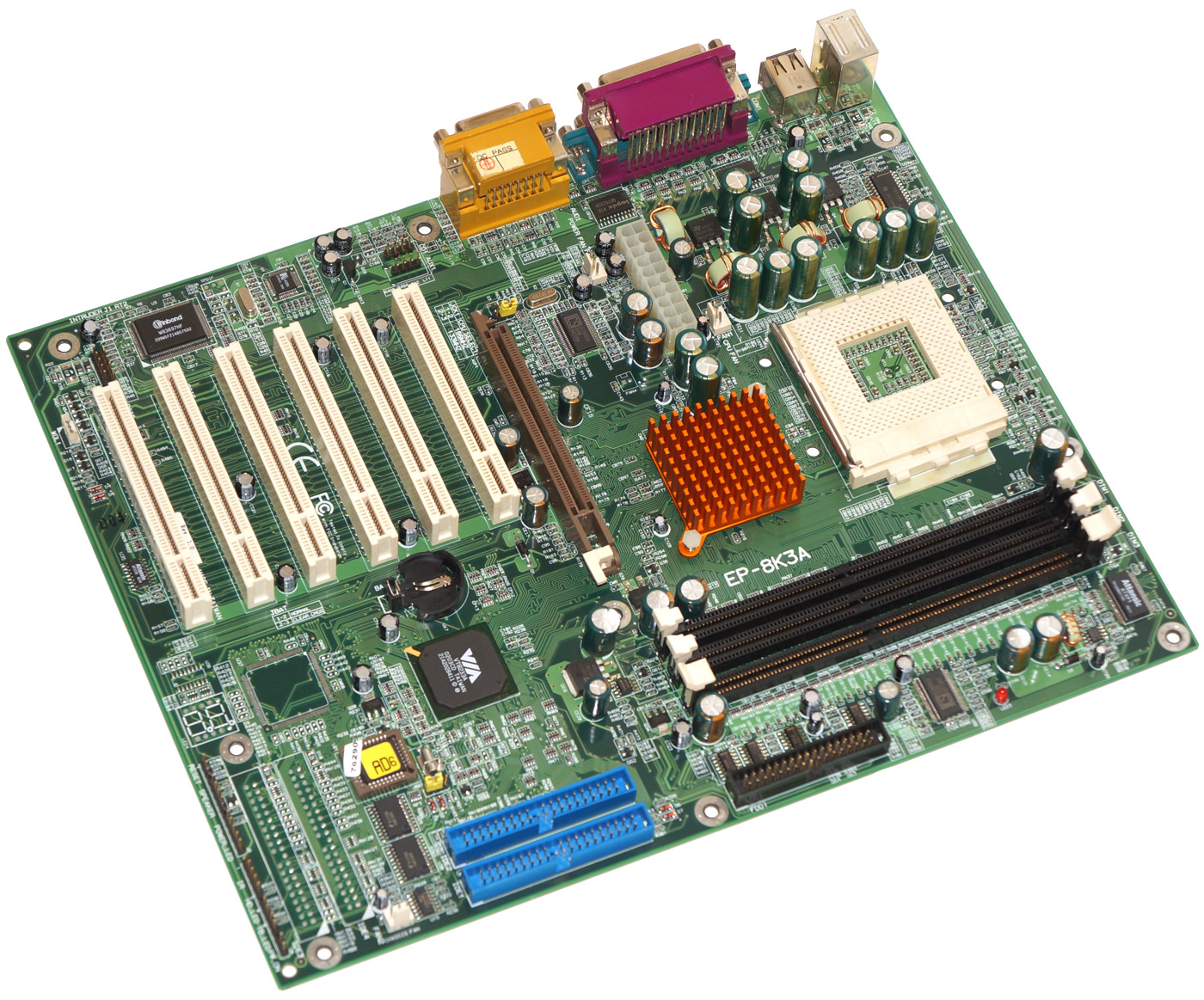
EPOX EP-8K3A, VIA KT333 chipset
Among the voltage regulation options, there is Vcore adjustment up to an impressive (and frightening) 2.2 V and Vmem up to 3.2 V, but the board lacks the possibility of increasing voltages for the chipset and AGP. The multiplier can be changed in the range from 6 to 15 in 0.5 steps, the FSB frequency can be overclocked up to 255 MHz in 1 MHz steps. One of the useful “chips” of the board is the presence of an automatic FSB – PCI divider, which can take a value of 1:5, which allows you to safely use FSB values above 166 MHz, at which the PCI frequency will be equal to the standard 33 MHz.
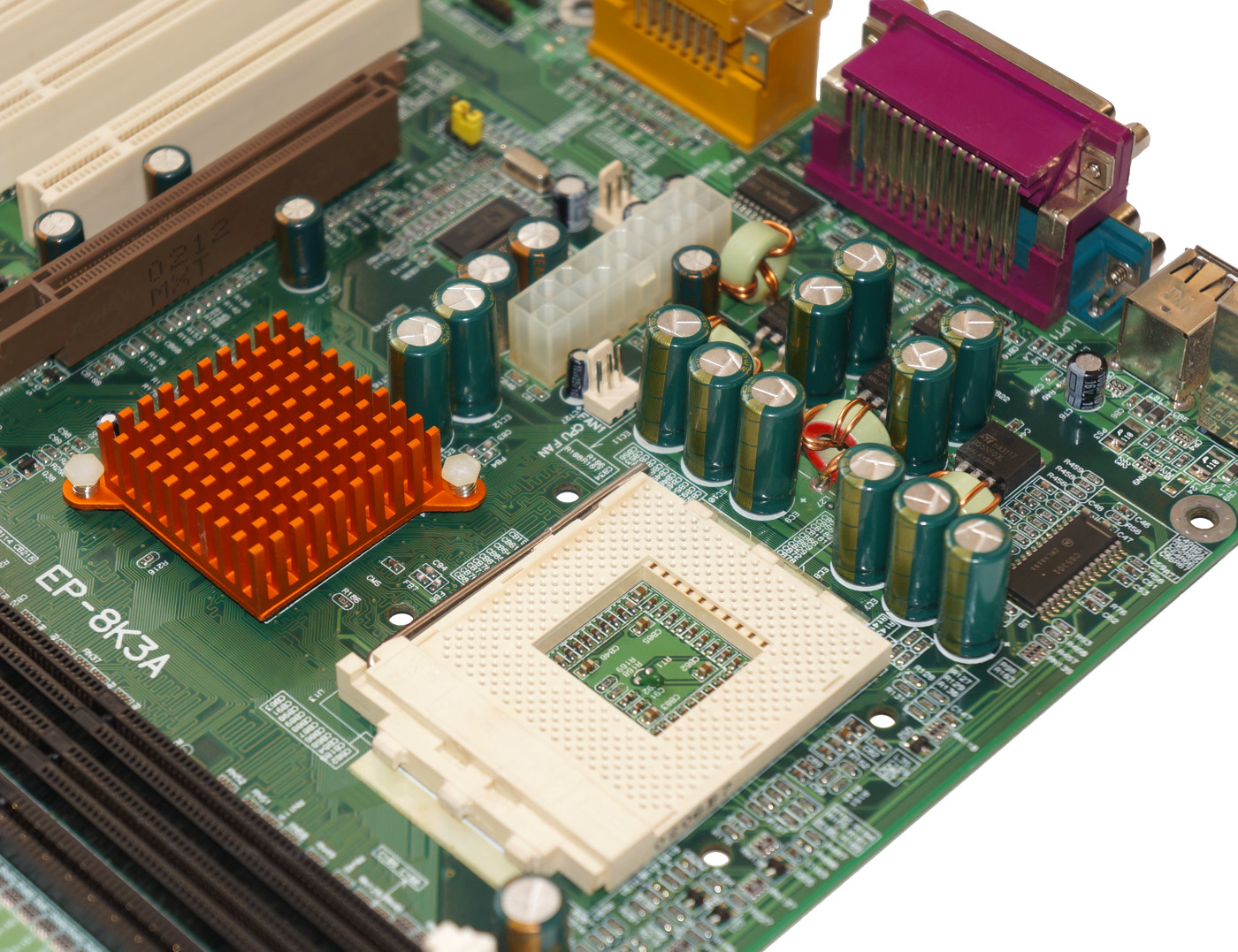
The North Bridge perhaps could use some active cooling.
The downside is the impossibility to set this divide manually. In other settings, the BIOS loses to the BIOS from ABIT, fewer settings for the CPU and memory subsystems, for example, the TRAS timing cannot be set to 5. If EPOX can be called an airplane, then ABIT is a rocket.
EPOX EP-8K9A7I – KT400A
The next participant will be a motherboard based on the VIA KT400A chipset, again from EPOX, the EP-8K9A7I. This model does not stand out in any special way, the physical dimensions of the board have decreased, one PCI slot has been removed, and in other respects it is almost like the previous EPOX, only the settings in the BIOS have become a little less.
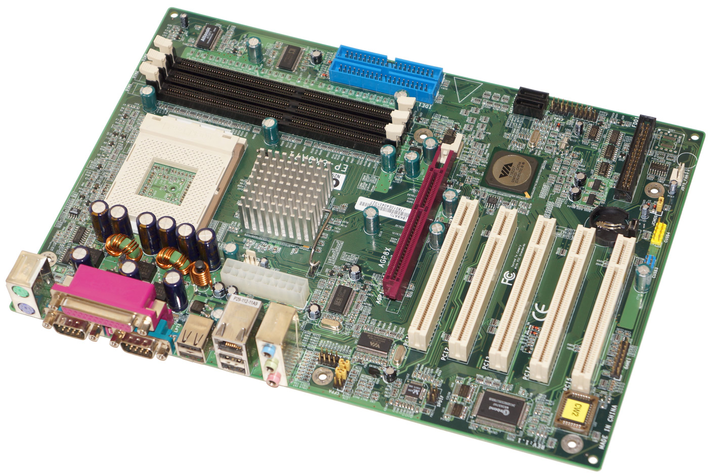
EPOX EP-8K9A7I, VIA KT400A chipset
But this motherboard is not positioned as a racing car, although for this testing and checking the performance of processors with a clock frequency of 1 GHz and a system bus of 100 and 133 MHz, its functionality, which is mainly determined by the VIA KT400A chipset itself, is quite enough. Compared to the previous generation of chipsets, the VIA V-Link bus, which connects the north and south bridges, has been updated to the second revision, the data exchange rate has increased from 266 to 533 MB / s. Added AGP x8 mode and support for single-channel DDR-SDRAM 400 MHz.
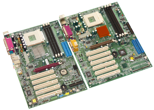
EPOX EP-8K9A7I on the left and EP-8K3A on the right
Of the features of this board, the TRAS = 5 timing cannot be set by tradition, plus the motherboard relies on its internal algorithms, and not on the preset settings in the BIOS, so with FSB = 133 (266) MHz and set 166 (333) MHz for memory, the Command Rate parameter from = 1 is automatically set to the value = 2. In general, not a rocket nor a race car, but adequate for testing.
EPOX EP-8RDA3I – Nvidia nForce 2 Ultra 400
The last participant in this test will be a motherboard based on the fastest nForce 2 Ultra 400 chipset for Socket 462. The EPOX EP-8RDA3I, familiar to many, will be used as a test sample, which was used by millions of users at one time and is not needed in a separate presentation.
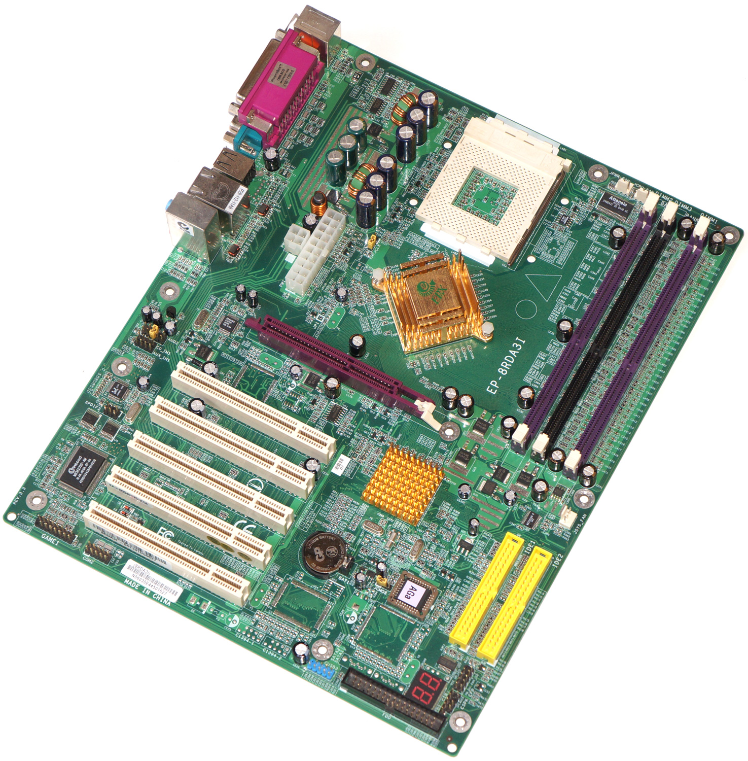
EPOX EP-8RDA3I, nForce 2 Ultra 400 chipset
It doesn’t make much sense to describe it in detail, the main thing is a fast chipset with a dual-channel DDR400 RAM mode. It’s time to move on to the tests themselves.
Article/Testing by Max1024, edited by CPUShack .
Part 2 – On to The Tests Already!