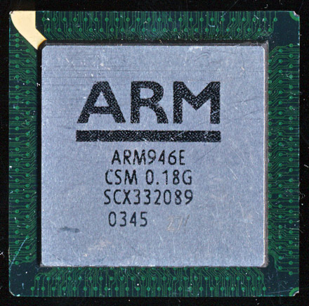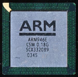
ARM946E on a Chartered Semiconductor 0.18u Process
ARM is one of the most popular RISC cores used today, and has been for over a decade now. ARM is an IP company. They license processor designs/architectures for others to use, but do not actually manufacturer the processors themselves….or do they?
ARM offers a variety of cores, and licenses them in a variety of different ways. There are, in general, three main ways to get an ARM design. Larger companies with may resources (such as Apple, Broadcom, or Qualcomm) will purchase an ARM architecture license. This isn’t specific to any ARM core in particular (such as say a ARM946) but the entire ARM architecture, allowing these companies to design their own ARM processors from the ground up. This takes a lot of resources and talent that many companies lack.
Second, ARM offers RTL (Register Transfer Level) processor models, these are provided in a hardware programming language such as VHDL or Verilog. They can be dropped into a design along with other IP blocks (memory, graphics, etc) and wrapped with whatever a company needs. This is a fairly common method, and typically the lest expensive. It does require more work and testing though. Designing a chip is only part of the process. Once it’s designed it still must be fab’d.
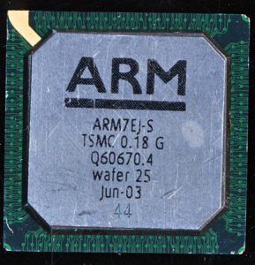
ARM7EJ-S on a TSMC 0.18u Process. Wafer #25 from June 2003
ARM also offers ARM models that are transistor level designs, pre-tested on various fab processes. Pre-tested means exactly what it sounds like. ARM designed, built and had them manufactured, fixing any problems, and thus giving the ability to say this core will run at this speed on this fab’s process. Testing and validation may often go as far as testing a particular fab’s particular process, in a particular package. Its more work, and thus cost more, but these make for drop in ARM cores. Want to use a ARM946 core, on a TSMC 0.18u process in a lead free Amkor BGA package? Yah ARM’s tested that and can provide you with a design they know is compatible. This allows extremely fast turn around from concept, to design to silicon.
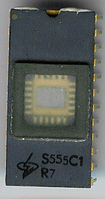
In the below picture (click to enlarge) you can see a large variety of ARM cores from the early 2000’s. They span ARM7, ARM9, ARM10 and ARM11 designs. Each is marked with info as to what exactly it is. The core name, the revision (such as r2p0, meaning major revision 2, pass/subversion 0) as well as the Fab (TSMC, UMC, SMIC, Chartered) and the design node (all of these are either 0.18 or 0.13u processors).
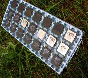
21 Various ARM design tet chips from TSMC, UMC, Charted, covering many ARM cores.
Also noted on some is the exact wafer the die was cut from, this is typical on VERY early production tests, usually first run silicon, so they can identify any physical/manufacturing defects easier. Some design modifications have little to do with the processor itself, but are done to increase yields on a given process/node.
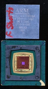
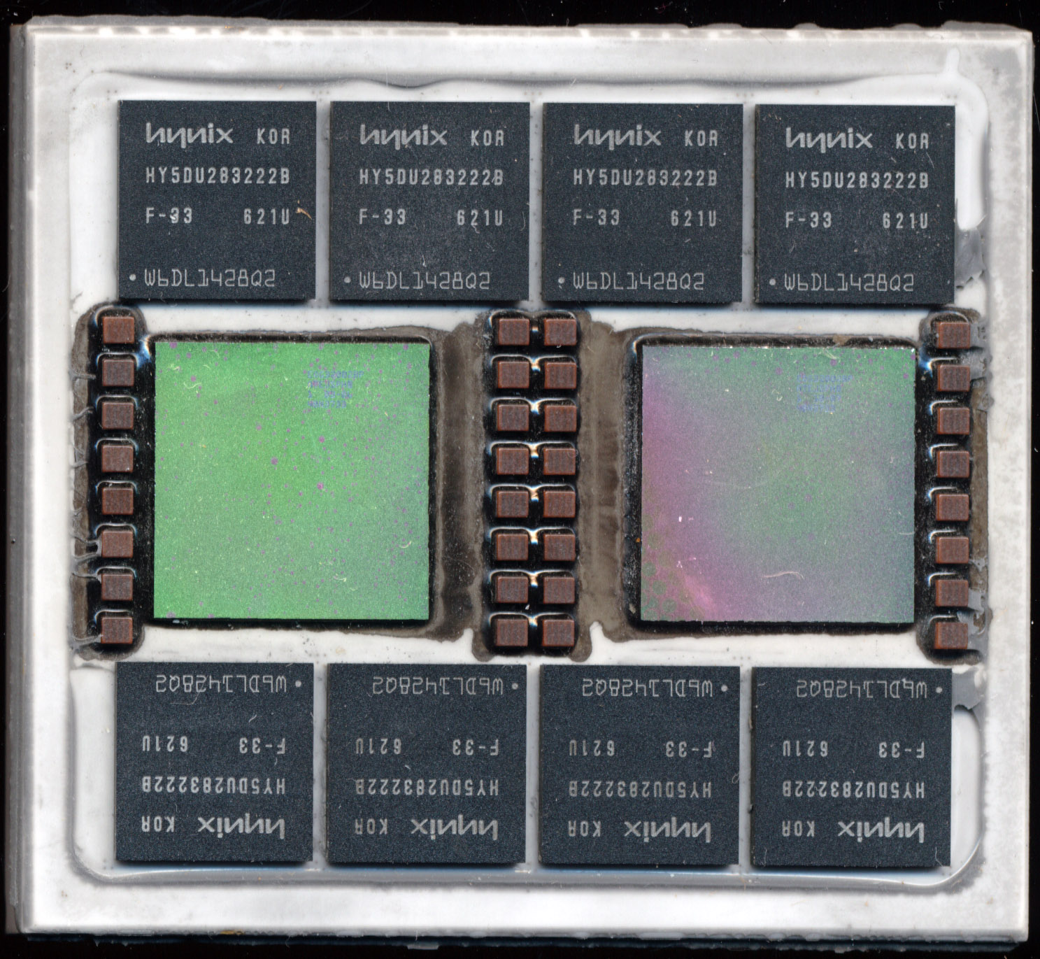
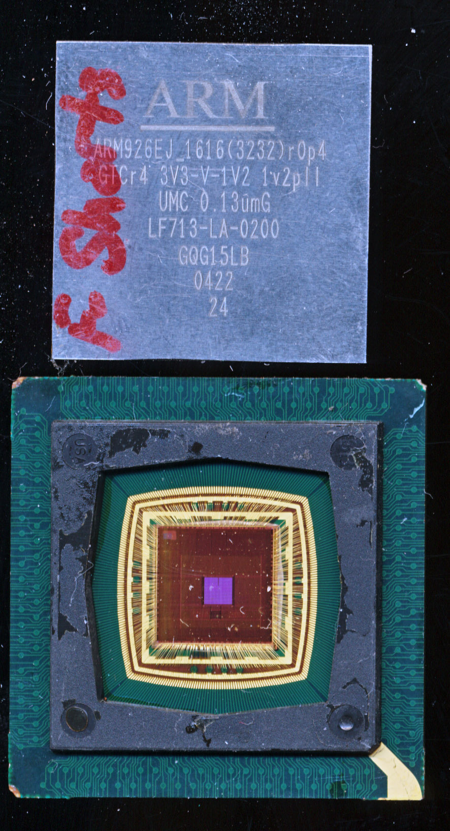
ARM926EJ on a UMC 0.13u Process.
Package type (in this case most are Amkor BGA) and other features are noted. Many say ‘ETM’ which is ARM’s Embedded Trace Macrocell, a debugging tool that allows instruction and date traces of an in operation core, very useful for debugging. ARM offers ETM for each of their processor types (ETM9 for example covers all ARM9 type cores) and itself has a revision number as well.
Some of these chips come in an interesting BGA package. The package has a removable die cover for inspection/testing (and possibly modification). Note the large die in the ARM926EJ on the left, though the processor core itself is very small (its in the upper left only a few square mm). This is done to facilitate bonding into the package, In this type of package there wouldn’t be any way to connect all the bonding wires to the very tiny ARM core, so the die has a lot of ‘wasted’ space on it.
So does ARM make processors? Yup! but only for internal use, to help develop the best possible IP for their clients.