
The Forgotten Ones: Actron AM1608 16-bit CPU.
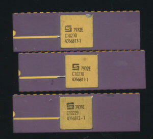
AM1608 Chipset – 1979 – Synertek
Back in 1974 the US Air Force saw the beginnings of a problem as the switch to digital microprocessor controls took over. “Fearful of being stuck with many unique systems requiring extensive software and hardware
support, the Air Force Aeronautical Systems Division (ASD) wants a standard device that could be applied across the board.” Sounds Familiar? (this same problem is what ended up leading to the MIL-STD-1750A processor indirectly). At the time though, this was an AIr Force only project (other branches of course had their own). The USAF called their ‘standard’ the UDAM, for Universal Digital Avionics Module. Like the 1750A, it was to be a standard, not an architecture, companies could create whatever architecture they wanted, however they wanted, as long as it met the standard. McDonnell Douglas (MD), at the time a huge contractor for the Air Force (as well as civilian airplanes) decided to make an entry. MD had a captive company since 1972 called Nitron to manufacture any semiconductors that MD needed for their various planes etc. Nitron was famous for their work on memory (notably EAROMs) but they could make most anything. MD also had another division called Actron (in Monrovia CA) , Actron designed boards and chips for MD, and then Nitron fab’d them. Convoluted, but such is the nature of such large organizations.
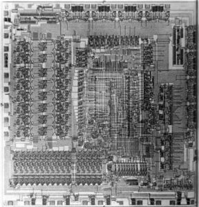
Control Chip DIe – AM1608 – Should be Nitron production.
The design Actron came up with went into production in early 1975 as the AM1608 at Nitron’s fab in Cupertino California. It was a 16-bit design (which was the requirement) implemented in 3-chips. There was a control chip, and a pair of identical 8-bit arithmetic chips. Essentially a bit-slice design, as was fairly common in the 1970’s. The AM1608 had a fixed 16-bit instruction length but data words could be used from 8-80 bits. Actron hoped they could use/sell this design for more than just the Air Force UDAM project.
The chips were initially fab’d on a 5-micron NMOS process with the control chip having ~4413 transistors on a 25mm2 die. Details on the arithmetic chip are unknown. They could execute around 200,000 instructions per second at a 2-2.5MHz clock. ADD/SUB took around 0.8microseconds with a worst case MULT instruction taking 6.8 microseconds. These processors’ were designed primarily for math, similar to the GA-16 from General Automations. Each 16-bit processor could address 8k 16 bit words of instruction ROM. It was expected that the design would move so a silicon gate CMOS process which would double its speed.
Posted in:
CPU of the Day