Sushi Tacos and Lasers: Marking Intel Processors
Intel ink stamp used for marking chips in the 1970’s
In 1987 Intel became the first semiconductor manufacturer to use lasers to mark all component parts, including ceramic packages (they still used ink for some but had the capability and eventually rolled out laser marking to most all of their assembly/test locations). Conventional ink marking for ceramic packages required a post-mark ink cure time and production yields ranged from 96%-98% before rework. That percentage may be good on a school exam, but in the production environment, having to rework 2-4% of everything off the line is unacceptable. It costs resources, money and time that do not go to making profit.
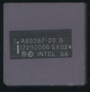
Intel A80387-20B SX024 remarked with a laser
With lasers, however, the cure operation was not needed and yields increased to better then 99.95%. Lasers were so consistent that marking became a zero rework process and overall productivity increased by 25%. Throughput also increased significantly (less rework and lasers are faster) and inspection requirements dropped by 95%. These lasers were originally developed for ceramic packages but found to work well on plastic packages as well. They also made remarking significantly easier, old markings could be crossed out with the laser and new marking made. No stencils, pads or masks were needed, the lasers were programmable and very fast.
Intel continues to use laser marking today (as do most manufacturers). Intel uses laser marking systems from Rofin-Sinar (now owned by Coherent). These lasers are typically from the PowerLine E line, which are a diode end-pumped Nd: YVO4 (Neodymium doped yttrium vanadate) diode laser. These are basically a high ends high power version of the diode lasers used in laser pointers. Intel went with diode lasers as they were faster, and cleaner then CO2
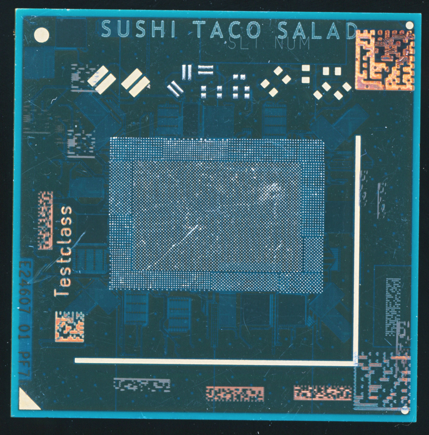
Intel Package marked SUSHI TACO SALAD. Perhaps the technician was getting hungry while trying to dial in the laser settings.
lasers (at the same power levels). These lasers typically run in the 10-40Watt range. Most commonly they are a 532nm laser (green light). In order to achieve the speeds needed, these marking systems are ran in a pulsed mode, 1-200KHz depending on the speed and material being marked. This allows the laser to run at very high power, for very short pulses.
This of course requires some tuning, essentially simple trial and error to find the right setting for a given material. Today’s packages are very thin, and marking on the organic substrate (or the silicon die itself) must be done in a way that leaves the markings visible, but does not damage the underlying structure. These markings are often only a few microns deep on silicon and 25 microns on a package, as deeper then th
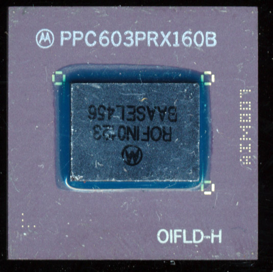
Motorola PP603 Engineering Sample with ROFIN BAASEL test marking on the die
at is the chips circuitry.
Rofin offers testing and calibration for some of their bigger customers (such as Intel) where they help develop the settings needed. This results in a lot of ‘oddly’ marked chips. Companies will ship packages, dies and whatever else needs to be marked to Rofin along with
specifications of the markings (how wide, tall, deep etc) and the systems/settings are worked out to make it workable on the production line. Anyone that has used a CO2 desktop laser knows they are not the fastest thing around. An engraving project completion time is measured in minutes. When marking chips, speed and accuracy are of paramount importance. Rofin advertises their lasers as such “Our semiconductor marking solutions achieve marking speeds up to 1600 characters/second. Even at a character height of 0.2 mm and line widths of less than 30 µm they still ensure best readability.”
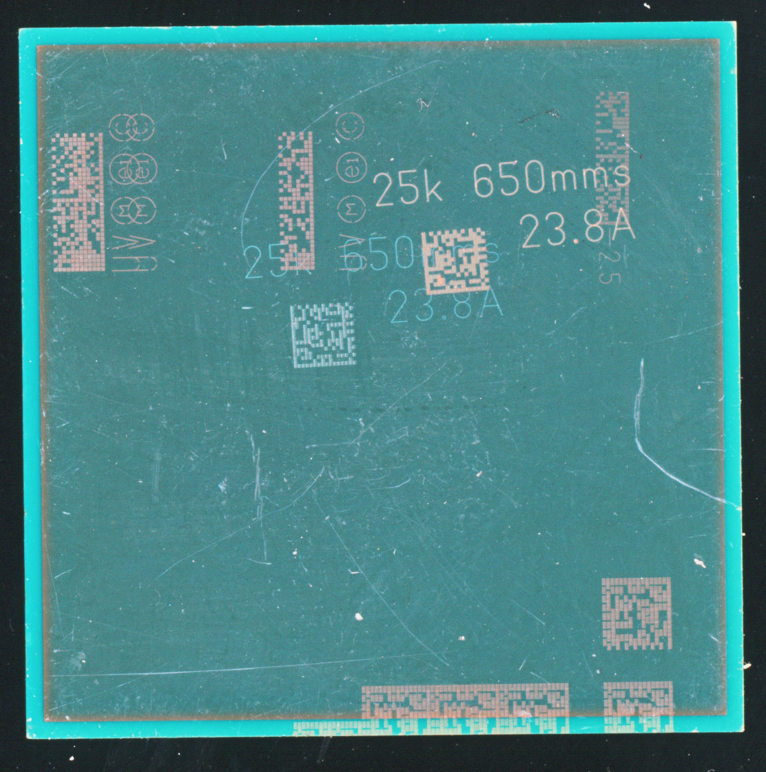
Package with laser settings engraved
Here we have a test chip package from Intel, marked up by Rofin, there is tests of the 3d-Bar code, Lots numbers s-specs and others. There is also some calibration markings, its useful to engrave the settings used as for the test, as the test. In this case we see 25k, 650mms and 23.8A. These are 3 of the fundamental settings for the laser system. 25k is the pulse rate (25KHz) of the laser, 650mms is the speed, or feed rate, 650mm per sec (about 2ft/sec), thats a relatively slow speed, but probably was one step in the calibration process. The 23.8A is the current for the laser, in amps. Its a rather high current compared to say a continuous wave CO2 laser which runs currents in the milliamps, but these are pulsed lasers, so that current is only needed for a fraction of a second.
Marking can also be done on the die itself. Here we see a sample
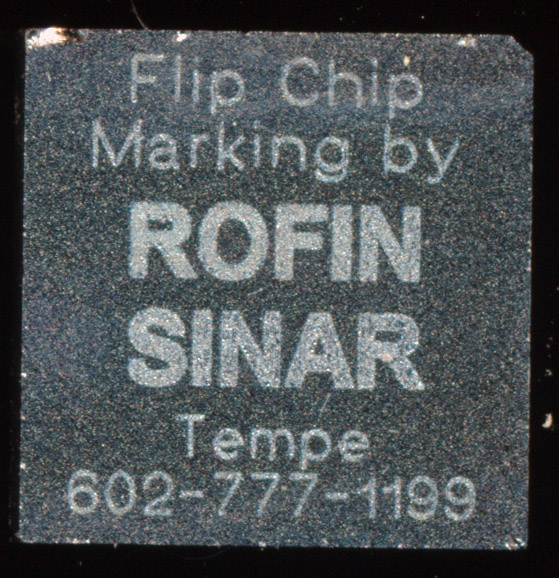
Flip chip marking marketing sample by ROFIN SINAR in Tempe, AZ
(probably an actually marketing sample given away to customers) of a flip chip die, with ROFIN SINAR markings on it, and erven their phone number for their location in Tempe, AZ (only a few miles from several fabs in Chandler, AZ (including Intel and Motorola (now NXP)).
As chips become smaller, marking technology continues to evolve with it. Markings today have become much less about what the consumer sees, and much more about traceability and trackability. Being able to follow a device through the supply chain, or trace a defective device back to when/where it was produced. Marking enhancements also play a great role in combating counterfeiting, helping them out of the supply chain.
There is a lot that goes into designing, making, assembling and even marking a computer chip, and often times things that seem the simplest, such as placing marking on a chip, are anything but simple, and just as important as the fabrication of the die itself.
Posted in:
CPU of the Day