Archive for August, 2016

August 25th, 2016 ~ by admin

Intel i486 Prototype: Intel’s Gamble with CISC

Intel A80486DX SXE19 Engineering Sample - May 1989

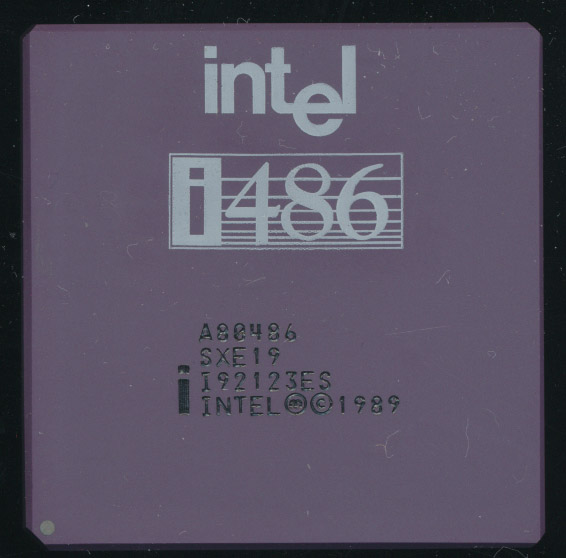
Intel A80486DX SXE19 Engineering Sample – May 1989

The Intel 80486 was announced at COMDEX in April 11th 1989, justy 3 years after the 80386 hit the market.  The 80486 was really a greatly enhanced 80386. It added a few instructions, on-chip 8KB Write-Thru cache (available off chip on 386 systems) as well as an integrated FPU.  Instruction performance was increased through a tight pipeline, allowing it to be about twice as fast as the 80386 clock for clock.  Like the 80386 the 80486 was a CISC design, in an era when the RISC processor, in its may flavors, was being touted as the future of ALL computing.  MIPS, SPARC, and ARM all were introduced in the late 1980’s.  Intel themselves had just announced a RISC processor, the i860, and Motorola had the 88k series.  Intel in fact was a bit divided, with RISC and CISC teams working on different floors of the same building, competing for the best engineering talent.  Would the future be CISC, with the 80486? Or would RISC truly displace the CISC based x86 and its 10 years of legacy?

This dilemma is likely why Intel’s CEO, Andy Grove, was nearly silent at COMDEX.  It was only 4 years previous the Mr. Grove, then as President, made the decision to exit the memory market, and focus on processors, and now, a decision would soon loom as to which type of processor Intel would focus on.  Intel eventually ditched the i860 and RISC with it, focusing on the x86 architecture.  It turns out that ultimately CISC vs RISC didn’t greatly matter, studies have shown that the microarchitecture, rather then the Instruction Set Architecture, is much more important.

Intel A80486DX-25 - SX249 - B4 Mask from Sept 1989 with FPU Bugs

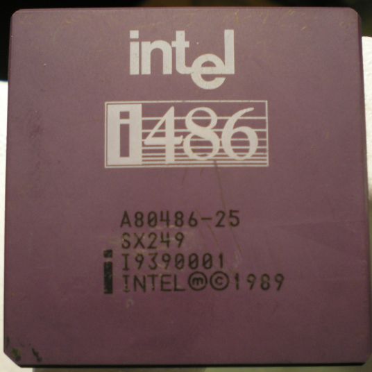
Intel A80486DX-25 – SX249 – B4 Mask from Sept 1989 with FPU Bugs

Whether due to the competition from the i860 RISC team, or knowing the markets demands, the 80486 team knew that the processor had to be executed flawlessly.  They could ill afford delays and bugs.  Samples of the 80486 were scheduled to be released in the 3rd quarter of 1989 with production parts shipping in the 4th quarter.  The above pictured sample is from May of 1989, a quarter ahead of schedule.  Production parts began to ship in late September and early October, just barely beating the announced ship date.

Perhaps due to the rush to get chips shipping a few minor bugs were found in the FPU of the 486 (similar to bugs found in the FPU of the 387DX).  Chips with the B4-Mask revision and earlier were affected (SX249).   These bugs were relatively minor and quickly fixed in the B5 mask revision (SX250), which became available in late November of 1989, still within Intel’s goal of the 4th Quarter.

The 80486 was a success in the market and secured CISC as the backbone of personal computing.  Today, the CISC x86 ISA is still used, alongside the greats of RISC as well.

August 19th, 2016 ~ by admin

CPU of the Day: Motorola MC6801 – The (second) first 6800 MCU

Motorola XC6801L - Early White ceramic package from 1979. XC denotes a not fully qualified part.

Motorola XC6801L – Early White ceramic package from early 1979. XC denotes a not fully qualified part.

A microcontroller (or microcomputer) is a CPU, with additional on-board peripherals, usually containing RAM, ROM, and I/O as to serve as a single (or close to single) chip solution for a computer system.  As the program space is typically small, they were designed and used for high volume, low cost, simple applications.  Today we would refer to them as embedded applications.  The Motorola MC6800, released in 1974 was a decent 8-bit processor.  It was however not inexpensive (a fact not lost upon one of its designers, Chuck Peddle, who left to design the 6502).  Initial pricing for the MC6800 was $360, dropping to $175 the next year.

For embedded use, prices needs to be in the few dollars range, with as little chips as possible required for a design.  By 1977 Motorola had a solution, the MC6802.  This MC6802 was an enhanced MC6800 128-bytes of RAM and an on-board clock-generator.  When combined with the MC6846 (which provided ROM, I/O and Timers) a complete system could be built.  Defective MC6802s were often sold as RAM-less MC6808s.

Motorola MC6802L - Dated March of 1978. The 6802 had 64-bytes of RAM and no ROM.

Motorola MC6802L – Dated March of 1978. The 6802 had 64-bytes of RAM and no ROM.

The MC6802 was followed by the more complex MC6801, which integrates the features of the MC6846 on die, making a true 8-bit single chip microcomputer.  Most sources refer to the MC6801 being released in 1978, however it was actually released in 1977, likely at the same time, or similar as the MC6802.  US Patent Application US4156867 filed on September 9th of 1977 references both processors.  GM was to be the lead customer for the MC6801, it was the MCU of choice for the digital trip meter (TripMaster) of the 1978 Cadillac Seville.  The 1978 Seville began production on September 29, 1977 on a 5.1um NMOS process.  It is likely that all of the first production of the 6801 was reserved for GM, and it wasn’t until 1978 and later that Motorola began to market it (it begins to show up in Motorola marketing only in 1979).  In 1979 the MC6801 also switched to a 3.9um HMOS process, which likely increased yields and decreased costs.  The TripMaster was a $920 factory option that proved to be rather unpopular, likely due to it adding nearly $1000 in cost to a $14,000 car.

Motorola MC68701U4L-1 1987 6801 with upgraded RAM/ROM and Timers

Motorola MC68701U4L-1 1987 6801 with upgraded RAM/ROM and Timers

This lack of early availability, coupled with the fact that while capable, the 35,000 transistor 6801 wasn’t particularly inexpensive led it to have very little success in the market.  The EPROM version, the MC68701 infact is much more common, likely due to the fact that it was used in lower volume products, where cost wasn’t such an issue.  In 1979 Motorola attempted to remedy this by releasing the MC6805 series.  This was designed from the ground up to be low cost.  The first versions had half the ROM and half the RAM as the 6801, while keeping the I/O.  They were also available in CMOS (as the MC146805).  They were inexpensive, and highly functional, and were widely used.  The 6805 continues to see use today as the 68HC05 and 68HC08 series.

Motorola XC68HC11A0FN - 1987 - Preproduction, Enhanced 6801

Motorola XC68HC11A0FN – 1987 – Preproduction, Enhanced 6801

The MC6801 was not, however, done.  By this time manufacturing had improved, allowing costs to be lower.  Motorola released an upgraded 6801, the MC6801U4 which expanded the timer functions, increased the ROM to 4K, and increased the RAM to 192-bytes.   In 1985 the MC6801 was upgraded again, a second 16-bit index register was added, as well as true bit-manipulation instructions.  The Motorola MC68HC11, the name change reflecting the greatly enhanced core, was made in many varieties with different sizes of RAM, ROM, and EEPROM. The MC68HC11A8 was also the first MCU to integrate EEPROM on die, in this case, 512 bytes worth.  The MC68HC11 series, and its 68HC12 and 16 successors, continue to be made, and used today, ironically, frequently in automotive applications, where the original MC6801 failed to be a success.


August 8th, 2016 ~ by admin

Intel MCS-86 Test Systems now available.

MCS-86 Test Boards For SaleThe CPU Shack is pleased to now offer test systems for testing the famous Intel 8086 and 8088 processors.  They also support testing of the 8087 FPU, as well as the NEC variants (V20/V30).  As an added bonus, an expansion is included for testing the i186/i188 processors as well.

Of course the original NMOS,  and later CMOS versions are supported from many manufacturers.

Head on over to the MCS-86 Test System page for more information and to order your system.


Posted in:
Products