Archive for March, 2013

March 27th, 2013 ~ by admin

Just for Fun: Wafers – Lots and lots of Wafers

Here at the CPU Shack I handle shipping and receiving for collectors all over the world, this means i have packages coming in daily, dozens of them.  Sometimes collectors will go in together to get a large lot of processors etc.  Today one such lot arrived, over 2200 wafers from Kokomo Semiconductor.  That’s nearly 300lbs.

Packages

Noel, the CPU Shack’s head of security, does not seem impressed.

Posted in:
Just For Fun

March 23rd, 2013 ~ by admin

Intel Pentium Processor Turns 20 Years Old

Intel Pentium 60

Intel Pentium 60 – Produced May 1993

On March 22nd, 1993 the Intel Pentium Processor was released to the public (so yah yesterday but hey whose counting). This was Intel’s first processor with an actual name.  Turns out you cannot trademark a number, so the ‘486’ name was being used by everyone (AMD, Cyrix, TI, UMC, IBM etc).  Initially known by its core name, P5, the Pentium was also the first superscaler Intel x86 processor   It had dual Integer pipelines, and a single Floating point unit allowing it to issue and complete multiple instructions per clock.

The first Pentiums ran at 60 and 66MHz and were made on a CMOS 0.8micron process with 3.2 million transistors.  After only a few months it was discovered that they ran particularly warm and the package was updated with a Copper-Tungsten heatspreader (gold plated).

A modern desktop processor such as the Core i7 Quad Core Ivy Bridge contain 1.4 Billion transistors on a 22nm process.  The P5 still lives on in the embedded market, and in the Intel Larrabee project which is itself, an updated P54C core (supporting a few more modern features such as x86-64).

Tags:
,

Posted in:
Just For Fun

March 22nd, 2013 ~ by admin

CPU of the Day: IBM Micro/370 – True Mainframe on a chip

IBM System/370 - 1970

IBM System/370 – 1970

IBM introduced the 12.5MHz cabinet sized System/370 in June 1970 as an evolution of the System/360 from 1964.  These systems formed the entire base of IBM’s mainframe business.  Today’s System z, itself an evolution of the original System/360 and 370, can still run many of the original programs, unmodified, from 50 years ago.  This is a testament to 2 things, the wide adoption of the IBM systems, and the forward thinking of IBM.  Even the original System/360 from 1964 was a full 32-bit computer.  Single chip processors did not embrace 32 bit architectures until the very early 1980’s (Motorola 68k, National 32k, etc).

In 1980 IBM sought to make a single chip version of the 370, in an effort to make a version that could be used for desktop type computers.  This was to become the Micro/370.  There were 2 distinct products to come out of this goal that are widely confused and debated.  The first became the PC XT/370, an add in card(s) for an IBM PC to give it the capability to run System/370 software.  Later another version was developed called the Micro/370 as a single chip solution.

The PC XT/370 began as an experiment,  a test bed implementation of the System/370 in a microprocessor environment.  The goal was not to rebuild the 370 from the ground up (that would come later) but to merely implement its instruction set into an existing design.  The base processor had two main requirements:  it had to be 32 bits, and it had to be microcoded.  IBM’s engineers in Endicott, NY selected the then very new Motorola MC68000 processor as their basis.  It was one of the only 32-bit designs at them time so that no doubt helped in the selection process.

Read More »

March 16th, 2013 ~ by admin

ALU of the Day: Motorola MC14581CL – Logic 4 bits at a time

Motorola MC14581CL 4-bit ALU

Motorola MC14581CL 4-bit ALU – 1973

At the heart of every processor is an ALU, an Arithmetic Logic Unit.  It is what does the addition, subtraction, compares, and other logic function on the bits we call data. Add some memory for registers, stack, and program control and one has a basic processor, or bit slice processor.   In the 1970’s and even the 1980’s many systems still implemented their ‘processor’ in discrete logic.  The 74181 (TTL), 10181 (ECL) and 14581 (CMOS) were the heart of many of them.  The ‘181 could handle any of 16 arithmetic and logic functions on a pair of 4 bit words.

The Motorola MC14581CL was the first of the CMOS ALU’s.  This example was made in early 1973. CMOS itself was only patented a few years prior (1967) and didn’t see extensive use in processors until the mid 1970’s (RCA 1802) and most other processors in the 1980’s.  Remarkably, after 40 years, its still in its original package.

Tags:

Posted in:
CPU of the Day

March 13th, 2013 ~ by admin

IBM 3081 TCM Miniature Pendant

IBM 3081 TCM Pendant

IBM 3081 TCM Pendant

A few times I get things that are not processors but are memorabilia and are pretty special nonetheless.  Today these nice IBM pendants came in.  They are very small, measuring barely 37mm square but they weigh an impressive 60 grams.  They are a near perfect miniature version of a not so miniature IBM TCM (Thermal conduction module).  The 3081 TCM contained the cooling, and a very large MCM used in the 308x mainframe series (made from 1980-1987).  Each MCM contained up to 133 dies on a very large ceramic substrate with up to 16,000 contacts for the dies.  They were capable of speeds of up to 38MHz.  Each TCM was liquid cooled and dissipated around 300 watts of heat. A typical 308x system had 2 dozen of these.

A similar IBM MCM can be seen here: (a 9121 processor)

Tags:
,

Posted in:
Just For Fun

March 10th, 2013 ~ by admin

CPU of the Day: Intel RUPI-44 The 8051’s lesser known cousin

Intel C8744-8 Engineering Sample - Early 1983

Intel C8744-8 Engineering Sample – Early 1983

In 1980 Intel released the MCS-51 family of microcontrollers, a design that would go on to become one of the pillars of the 8-bit MCU market.  Initially the family consisted of the 8051, which included 4KBytes of on-chip ROM (or UV-EPROM in the case of the 8751) and 128 bytes of RAM as well as the 8031 which did not include the ROM, all program memory was off chip.

The 8051 was a wild success with Intel struggling to meet demand.  Intel did not have the fab capacity to produce both the 8051, and the very in demand 8088 (thanks to IBM).  In 1984 Intel opened a new fab in Albuquerque, New Mexico to build other chips, freeing up production space in the California fab for more 8051s.  Even so, an $8 8051 was routinely scalped for over $200 on the grey market and waiting periods of up to a year were common in order to receive orders, with many companies on allocation.  Intel licensed the design to both AMD (who built a fab in Austin to make it) as well as Signetics in an effort to keep up with demand.  The hardest to get part in the industry, was the 8051 from 1983-1984.

P8344 - A ROMLess 8044, so essentially an 8031 + SDLC controller.

P8344 – A ROMLess 8044, so essentially an 8031 + SDLC controller.

So in the midst of this insatiable demand for an MCU that they did not have the capacity to produce, Intel releases the RUPI-44 (Remote Universal Peripheral Interface). The RUPI-44, also known as the 8044, is an 8051 with an additional 64 bytes of RAM and a full serial communication co-processor on die.  Specifically it was an 8051 that handled the SDLC (Synchronous Data Link Control) protocol in hardware.  Intel had an SDLC controller, known as the 8273, but it was limited to 64kbps, the 8044 could handle data transfers of up to 2.4Mbps due to the 8051 core’s high speed and close coupling of the serial controller.

SDLC was developed in 1975 by IBM and was generally used as a way for mainframes to communicate with various peripherals and terminals.  It supports error correction and multi-point, point to point, and loop connections.  In 1979 SDLC was standardized as HDLC (High-Level Data Link Control) which the RUPI-44 also supports.  While popular in the 70’s and 80’s its use has faded out, though it achieved some long lived use in Europe running the Intel derived BITBUS protocol well into the 90’s.

Read More »

Posted in:
CPU of the Day

March 7th, 2013 ~ by admin

PENTIUM License Plate: One in a million, or 2

Original PENTIUM California License (number) plate

Original PENTIUM California License (number) plate

This California license plate came through the museum on its way to a collector in Sweden.  I get many items in that are unusual and rare but this was the first processor relates plate I have seen.  The best part? It came with some history.

It was ordered as a vanity plate by a salesman at Intel around 1995.  He was later hired by AMD as a sales person but his car still said “Pentium” which obviously was a bit of a problem.  As a token of commitment to his new company he gave it to his manager at AMD, despite the fact that he was offered $3000 for it from an employee at Intel.  It likely sat on a desk for some time until it was sold on eBay (for the low price of $100) where it was spotted by a collector in Sweden who asked me to purchase it for him.

It now resides with the collection of CPU Collection.SE

Posted in:
Just For Fun

March 2nd, 2013 ~ by admin

Chuck Moore: Part 2: From Space to GreenArrays

Part 2 of my abbreviated biography of Chuck H. Moore’s processor designs.  Part 1 covered the early days of Novix, and the RTX2000.

Patriot Scientific IGNiTE - Based on the Sh-Boom

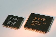
Patriot Scientific IGNiTE – Based on the Sh-Boom

Moore was not content to just create one processor design, or one company.  In the 1980’s he also ran Computer Cowboys, a consulting/design company.  In 1985 he designed the Sh-boom processor with Russell H. Fish III.  This was a 32-bit stack processor, though with 16 general purpose registers, that was again designed with Forth in mind.  It was capable of running much faster then the rest of the system so Moore designed a way to run the processor faster then the rest of the board, and still keep things in sync, innovative at them time, and now standard practice.  The Sh-Boom was not a particularly wide success and was later licensed by Patriot Scientific through a company called Nanotronics, which Fish had transferred his rights to the Sh-Boom to in 1991.  Patriot rebranded and reworked the Sh-Boom as the PSC1000 and targeted it to the Java market.  Java byte code could be translated to run in similar fashion as Forth on the PSC1000 and at 100MHz, it was quick.  In the early 2000’s Patriot again rebranded the ShBoom and called the design IGNITE.  Patriot no longer makes or sells processors, concentrating only on Intellectual Property (Patent licensing).

After designing the Sh-Boom, and the Novix series, Moore developed yet another processor in 1990 called the MuP21.  This was the beginning of a what would be a common thread in Moore’s designs.  MISC (Minimal Instruction Set Computer), which is essentially an even simpler RISC design, multiprocessor/multicore, and efficiency have become the hallmarks of his designs.  The MuP21 was a 21 bit processor with only 24 instructions. At 20MHz performance was 80 MIPS as it could fetch four 5-bit instructions in a 20 bit word.  It was manufactured in a 40 pin DIP on a 1.2 micron process with 7000 transistors.

iTvcIn 1993 Moore designed the F21, again a 21 bit CPU based on the MuP21, designed to run Forth, and including 27 instructions.  It was fab’d by Mosis on a 0.8u process.  The F21 microprocessor contains a Stack Machine CPU (with a pair of stacks like the NC4000), a video i/o coprocessor, an analog i/o coprocessor, a serial network i/o coprocessor, an parallel port, a real time clock, some on chip ROM  and an external memory interface. Performance was 500 MIPS (this was an asynchronous design, so ‘clock speed’ is a bit of a misnomer) and transistor count had risen to about 15,000.  The F21 was made up through 1998, however the design continued to evolve.  A version of the F21 was developed called the i21, originally for Chuck Moore’s iTV Corporation, which was one of the very first set top Internet appliance companies.  It integrated additional featured such as infrared remote interface, modem DMA interface and a keyboard DMA interface. The F21 scaled well, and was tiny, remember, only 15,000 transistors, which at 0.18u takes up a VERY small die, and allowed performance to hit 2400MIPS @ 1.8V.  One could put a very large amount of these on a single die…..

Read More »

Tags:

Posted in:
Research