January 15th, 2016 ~ by admin

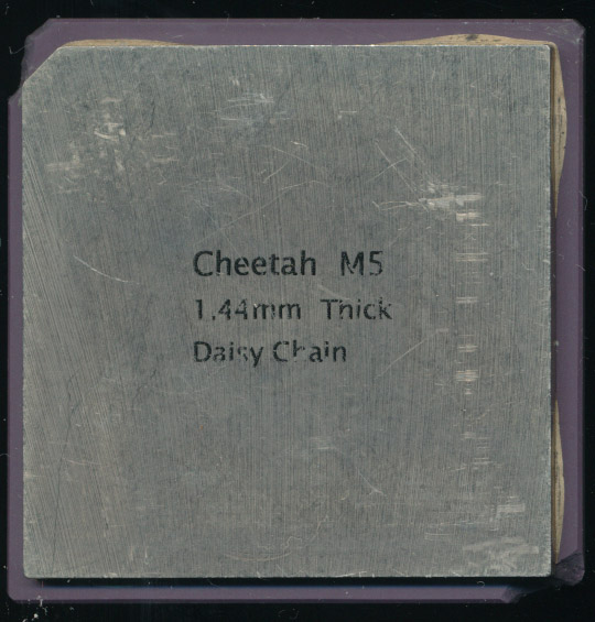
The Oracle SPARC M4 and how it became the M5 (but really didn’t)

Oracle SPARC M4 Wafer # 1 - No date, likely early 2011.

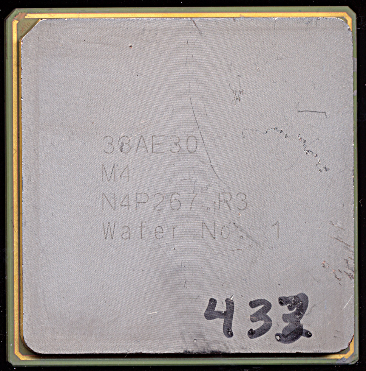
Oracle SPARC M4 Wafer # 1 – No date, likely early 2011.

The story of the Oracle SPARC M4 is best told starting with Afara websystems.  Afara was the original developer of the SPARC processor that became the SUn UtraSPARC T1, aka the Niagara.  Sun acquired Afara in 2002 in a sale that was really designed as a capital campaign for Afara, they had the technology and design for the processor, just not the money to enter the market, Sun had the money (or so they thought at the time).  The T1 was released in 2005 and had 4-8 cores.  The individual cores were called the SPARC S1 core (now an open source SPARC core).  In 2007 Sun released the Nigara 2, the UltraSPARC T2, with 4-8 cores, based on the second version of the S1, the S2.  Both the S1 and S2 were designed with multi-threading as the primary performance point.  They excelled at it, and the UltraSPARC T3, released in September 2010 (though it had been sampling all the way back in Dec. of 2009) did even better at multi-threaded applications.  The T3 also was fab’d by TSMC, a change from previous SPARCs which were almost entirely fab’d by Texas Instruments.

The T3, and the S2 core it was based on had one major problem. The S2 core had sub-par single thread performance.  While the workloads given to a SPARC server can be tailored somewhat to match was the processor does best (multi-threading) there is always going to be a point at which a single thread task must be done, and it will hold up the entire processor if it cannot be processed efficiently.

Read More »

Posted in:
CPU of the Day

November 8th, 2015 ~ by admin

Sun UltraSPARC IIIi+: The Serrano

Sun UltraSPARC IIIi+ Early engineering sample from August of 2005

Sun UltraSPARC IIIi+ Early engineering sample from August of 2005

In early 2004 Sun Microsystems had a lot going on.  The UltraSPARC IV had been announced, and Sun was already talking about its upgrade, the UltraSPARC IV+.  Sun had recently released the Jalapeno, aka the UltraSPARC IIIi, their second processor with on die L2 cache (The first being the IIe designed for embedded use) in 2003. In 2002 Sun had purchased Afara Websystems for their SPARC design, known as Niagara, which became the Sun T1, and were working on its successor, the T2.  Both the T1 and the UltraSPARC V (the successor to the not even itself yet released IV) was scheduled to tape out the next year, yet itself was canceled in April of 2004, most of the entire engineering staff working on it is laid off.

At the same time Sun was talking up an upgrade for the lower end UltraSPARC IIIi, this would be a relatively simple process, more the existing core to a new process.  It currently was being made by TI on a 130nm 7-layer Cu interconnect process with low-k dielectric.  Moving it to TI’s 90nm process would allow for greater clock speeds, less power, and room on die to quadruple the L2 cache to 4MB.  The processor was code named Serrano, and widely announced as an upgrade to Sun’s Fire V215, V245 and V445 servers. Sun promised a release in late 2005. And then…

Sun UltraSPARC III Cheetah - Early Mechanical Sampele.

Sun UltraSPARC III Cheetah – Early Mechanical Sample. The IIIi added on die L2 cache

Nothing, talk of the Serrano went silent, all PR focus has shifted to the coming T1 and the UltraSPARC IV+. Both are released in 2005 to great applause, but the tech community is still wondering where the IIIi+ has gone?  Sun isn’t exactly forthcoming as to why, mentioning that it had been delayed in order to get the T1 out the door.  In mid-2006 a customer commented, “There have been problems getting the UltraSPARC IIIi+ processors, so the new systems will be released with the current chips.”  Finally in August of 2006 Sun come forward and says that the IIIi+ has been canceled, but there is a catch, it was canceled the year before, and Sun decided to just keep mum about it.

Keep in mind the IIIi+, other then the increase in L2 cache, was a fairly ‘routine’ port to a new process.  The delays, and cancellation at the time sounded like it was due to technical grounds, but looking back, and seeing that they had working silicon in 2005, it would seem that the decision to kill the Serrano was resource driven.  Likely a combination of Sun’s engineering and marketing constraints, as well as the availability of the 90nm process at TI, which was also being used for the Niagara.

Manufacturing capacity is a finite resource, so not using up what may have been a very limited amount of fab space, on a processor that was designed to slot into the low end servers, is possibly the best explanation we have for the cancelling of the UltraSPARC IIIi+, perhaps a former Sun engineer can fill in some more details, as so many of them were laid off whom had worked on Sun’s previous processors.  It was a gamble by Sun, and one which seems to have paid off, considering the success of the Niagara, though Sun/Oracle were far from done with canceling designs, Honeybee, Rock, and M4 all come to mind.

Posted in:
CPU of the Day

July 26th, 2015 ~ by admin

Sun CoolThreads UltraSPARC T1 Sample

Sun UltraSPARC TI Marketing Sample

Sun UltraSPARC TI Marketing Sample

The Sun UltraSPARC IV consumed 105 Watts at 1350 MHz.  This for a dual core processor that could process 2 threads.  Sun decided that the T1 (aka the Niagra) was going to change that.  It was the first ground up redesign of the SPARC core since the UltraSPARC III.  Interestingly Sun originally first attempted to develop a multithreaded process by using a pair of UltraSPARC II cores on a single die.  That project was canceled in 2004, as the T1 was in development.

The T1 was designed to focus on maximum processor utilization.  It contained up to 8 cores, each of which could process 4 threads.  This allows the processor to be used more efficiently, as a single thread can not slow down the entire processor.  All 8 cores share a single Floating Point unit.  This worked well for most database type processing, as FP instructions are not very common in that type of computing.  The T2 (made on a smaller process) allowed for a FP unit for each core which allowed better performance in HPC applications.

Made by TI on a 90nm process, the T1’s 279 million transistors consume only 72 Watts, a 30% reduction from the UltraSPARC IV at a similar clock speed.  This is what Sun called CoolThreads Technology.  Released in November of 2005 Sun was a bit ahead of their time, lower power, more efficient processors were only just beginning to become an important selling point.  Interestingly, its sister project, the UltraSPARC Rk, turned out to be not so cool.  Today, 10 years later, energy efficiency is one of the key metrics when measuring processor performance.  With data centers having on average 50,000 computers, 30 Watts per chip adds up, quick.

Tags:
,

Posted in:
CPU of the Day

January 16th, 2015 ~ by admin

Sun UltraSPARC Rock: When is a core not a core?

Sun SME1832ABGA PG 2.2.0 UltraSPARC RK - 2007 Sample

Sun SME1832ABGA PG 2.2.0 UltraSPARC RK – 2007 Sample

In 2005 Sun (now Oracle) began work on a new UltraSPARC, the Rock, or RK for short.  The RK was to introduce several innovative technologies to the SPARC line and would complement the also in development (and still used) T-series.  The RK was to support transactional memory, which is a way of handling memory access that more closely resembles database usage (important in the database server market).  Greatly simplified, it allows the processor to hold or buffer multiple instruction results (load/stores) as a group, and then write the entire batch to memory once all had finished.  The group is a transaction, and thus the result of that transaction is stored atomically, as if it were the result of a single instruction.

The RK also was designed as a 16-core processor, with 4 sets of cores forming a cluster.  This is where the definition of a core becomes a source of much debate.  Each 4-core cluster shared a single 32KB Instruction cache, a pair of 32KB Data caches, and 2 floating point units (one of which only handled multiplies).  This type of arrangement is often called Clustered Multi-threading.  Since floating point instructions are not all the common in a database system, it made sense to share the FPU resources amongst multiple ‘cores.’

The RK was designed for a 65nm process with a target frequency of 2.3GHz, while consuming a rather incredible 250W (more power than an entire PC drew on average at the time).

AMD A6-4400M - 2 'cores' with shared FPU and cache.

AMD A6-4400M – 2 ‘cores’ with shared FPU and cache – Piledriver Architecture

This should sound familiar, as its also the basis of the AMD Bulldozer (and later) cores released in 2011.  AMD refers to them as Modules rather then clusters, but the principle is the same.  a Module has 2 integer units, each with their own 16K data cache.  a 64K instruction cache and a single floating point unit is shared between the two.  The third generation (Steamroller) added a second instruction decoder to each module.

The idea of CMT, however, is not new, its roots go all the way back to the Alpha 21264 in 1996, nearly 10 years before the RK.  The 21164 had 2 integer ALUs and an FPU (the FPU was technically 2 FPUs, though one only handled FMUL, while the other handled the rest of the FPU instructions) .  The integer ALUs each had their own register file and address ALU and each was referred to as a cluster.  Today the DEC 21264 could very well have been marketed as a dual core processor.

The SPARC RK turned out to be better on paper then in silicon.  In 2009 Oracle purchased Sun and in 2010 the RK was canceled by Larry Ellison.  Larry Ellison, never one to mince his words said of the RK:  “This processor had two incredible virtues: It was incredibly slow and it consumed vast amounts of energy. It was so hot that they had to put about 12 inches of cooling fans on top of it to cool the processor. It was just madness to continue that project.”  While the Rock (lava rock perhaps?) never made it to market, samples were made and tested, and a great deal was learned from it.  Certainly experience that made its way into Oracle’s other T-Series processors.