October 16th, 2016 ~ by admin

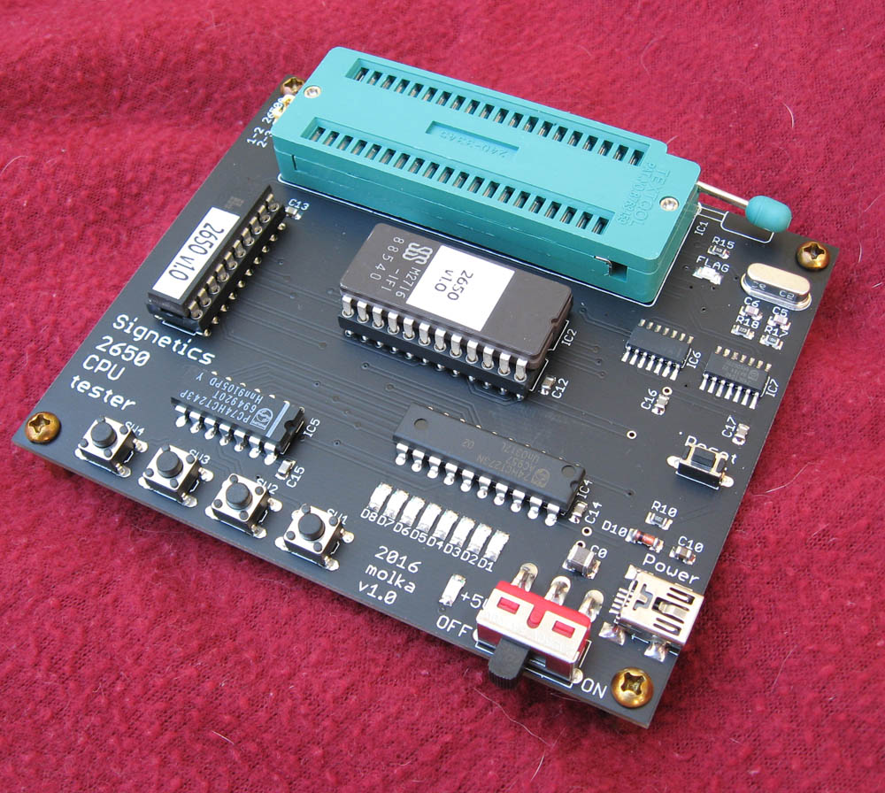
Signetics 2650: An IBM on a Chip

Signetics 2650I - Original Version from May of 1976

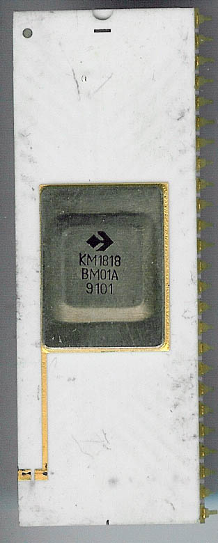
Signetics 2650I – Original Version from May of 1976

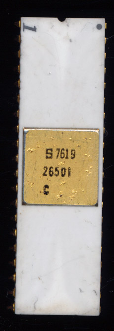
The Signetics 2650 processor has always been described as ‘very mini-computer like’ and for good reason, it truly is very minicomputer like in design.  It is an 8-bit processor released in July of 1975 made on an NMOS process.  The 2650 has a 15-bit address bus (the upper bit (16) is reserved for specifying indirect addressing) allowing addressing of up to 32K of memory.  It has 7 registers, R0, which is used as an accumulator, as well as 2 banks of 3 8-bit registers accessed.  The 2650 supports 8 different addressing modes, including direct, and indirect with autoincrement/decrement.  Its clearly a mini-computer design and there is a reason for that, it was based on one.

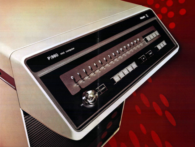
The 2650 is very closely based on the IBM 1130 mini-computer released in 1965.  Both use 15-bit addressing, many addressing modes, and a set of 3 registers (Signetics added support for 2 banks of 3,  The Signetics 2650 is often noted for its novel use of a 16-bit PSW status register, but this too is from the 1130, which used a 16-bit Device Status Register for talking with various I/O components.  So why would Signetics base a processor released in 1975 on a 1965 mini-computer?

Because the 2650 was not designed long before it was released.  J. Kessler  was hired by Signetics in 1972 in part to help design an 8-bit processor.  Kessler was hired by Jack Curtis, (Of Write Only Memory fame) from…IBM. Kessler designed the architecture very similar to the IBM 1130 and Kent Andreas did the silicon layout.  The design contains 576 bits of ROM (microcode mainly), ~250 bits of RAM (for registers, stack, etc) and about 900 gates for logic.  Clock speed was 1.25MHz (2MHz on the -1 version) on a ion implanted NMOS process, very good for 1972 (this was as fast as the fastest IBM 1130 made), but Signetics was tied up working with Dolby Labs on audio products (noise canceling etc) and didn’t have the resources (or perhaps the desire) to do both, so the 2650 was pushed back to 1975.  In 1972 the IBM 1130 it was inspired by was still being made.  If the 2650 had been released in 1972 it would have had the Intel 4004 and 8008 as competition, both of which were not easy to use, and had complex power supply and clocking requirements.  The 2650 needed a 5V supply, and a simple TTL single phase clock.

Read More »

Tags:
,

Posted in:
CPU of the Day

July 1st, 2016 ~ by admin

Signetics 2650 Test Boards Now Available

Signetics 2650 Test Board For SaleContinuing our goal of having test boards available for pretty much every common architecture of the 1970’s we now have a board available for testing Signetics (and later Philips) 8-bit NMOS processor, the 2650, 2650A and 2650B.  Made on a cool black PCB they are a fairly simple system, but are capable of testing some of the special features of the 2650 as well as the added features of the 2650B (if anyone happens to locate one)

These chips did not achieve the wide microcomputer success hoped for (likely due to a lack of second sourcing) they did find their way into many industrial/embedding systems, as well as many arcade/video games (including some made by ATARI).

These boards are in stock, and ship world wide for $94.95.  Head on over to the 2650 page to grab one.

Posted in:
Products

January 6th, 2016 ~ by admin

Signetics SPC-16/10: Another Mini goes Micro

Philips P860 Minicomputer - 1971

Philips P860 Minicomputer – 1971

In the 1960’s the Dutch Philips Data Systems marketed computers from Honeywell.  By 1970 they decided that simply reselling others machines was not the best value for them, or their customers and set off to design their own series of mini computers.  The first design was the 8-bit P410, which only saw limited success, it was a bit too mini for the early 1970’s when 16-bits or better was the standard. 1970 saw Philips begin work on its successor in Fontenay Aux Roses, near Paris, France, a project known internally as Sagittaire.  It was released in 1971 as the P800 series of mini computers, starting with the P850.   These were a 16-bit design, using 16 16-bit registers.  It shipped with 2k x 16bits of memory and had a cycle time of 3.2 microseconds (~312KHz).  Further versions were released that supported up to 32k x 16bits of memory and faster cycle times.

Philips P851 Chipset

Philips P851 Chipset

The P800 architecture used the A0 register as the Program Counter and the last register (A15) as a stack pointer.  The design supported up to 64 I/O devices and 64 interrupt levels.  The addressing modes include direct, register, indirect, indexed and indexed indirect types and can operate on bits, bytes (characters), words, and double words.  Since the stack is maintained in memory, the stack pointer can be rewritten, preserving the current stack for easier context switches.  This is of course important as the P800 is designed as a multi-user. multi tasking computer.  The P800 instruction set included 97 instructions, including MULT/DIV, though depending on the model, some of these were simulated (microcoded).  The P800 family found wide use in offices and eventually banks (always the big money market) throughout Europe.  It also proved to be useful in industrial environments, a somewhat underappreciated market for mini-computers at the time.

IRAS - Infrared Astronomical Satellite - Launched 1983 - Based on P851 chipset

IRAS – Infrared Astronomical Satellite – Launched 1983 – Based on P851 chipset

In 1979 Philips released the P851, a Single Board Computer (SBC), version of the P800 series.  It included the full 32k words of memory and was an LSI implementation using 5 Philips LSI’s consisting of 4 4-bit ALUs and a control path.  The P851 was used extensively for industrial automation as well as Philip’s own PM4400 computer system.  This system became the basis of the PM4421 development system which supported development and emulation of many processors, including the Intel 8085/86/88, Zilog Z80, 650x, Motorola MC68k, Signetics 2650 and many others.

The P851 LSI design was also used in space missions, perhaps the most famous in the IRAS mission launched in 1983.  This was the first full Infrared mapping mission launched, and in its 10 month mission, mapped almost the entire sky in 4 different IR wavelengths, IRAS Space Discoveries that are even today not yet identified.  The mission was of course limited by the coolant carried to keep the IR detector cold, but the IRAS satellite continues to orbit Earth to this day, with a 16-bit P851 computer still on board.

Read More »

October 20th, 2015 ~ by admin

CPU of the Day: Military Signetics 8X305 Processor

Signetics Military 8X305 - 1990 (8550201YA)

Signetics Military 8X305 – 1990 (8550201YA)

Some time ago we talked about the history of the Signetics 8X300 line of processors.  Originally released as the SMS300 in 1975 by SMS, the design was bought by Signetics.  It was a fairly unique 8-bit bipolar design, running at 8MHz. Its focus was signals processing, long before dedicated DSP’s such as the TI TMS320 came about.  The design was updated in 1982 to add some additional instructions and data handling.

Since it excelled so well at signals processing, the design worked well for military applications, where signals processing was of great use (interpreting data from a host of, usually, RF sensors.  The 8X305 was made in the normal 50 pin DIP, a 68 pin LCC, and an unusual 52 pin flat pack for military use.  In the 52-pin package the extra 2 pins are simply ‘No Connects’. (In the 68 pin version the extra 18 pins are divided amongst extra VCC, VR, GND, and N/C).

For military applications the greatest importance is on reliability.  This takes the form of three main areas:

Mechanical: How well can the design handle shocks, and vibrations, usually this is handled through better bonding wires, and more rigid package specs/inspection.
Electrical: How well can the device tolerate not great electrical conditions, higher reliability is achieved when the device can operate with a voltage that may very up to 10%, rather then the 5% or less commercial devices are designed to.
Temperature:  This is closely related to mechanical, as temperature stability requires the package to be damaged by expansion/contraction in wild temperature swings.  Obviously the silicon die itself needs to work with the same electrical characteristics at different ends of the temp range.  Many electrical parameters (such as resistance, and biasing) change over temperature, so the device must handle this. Typical military spec is -55C-125C (-67F-257F).  A range of 180C, from well below freezing, to well above boiling.

Venus - From the Mariner 10 Probe

Venus – From the Mariner 10 Probe

This Signetics 8X305 (Drawing # 8550201YA) is rated at -55-125C at 5V +/- 10% running at 8MHz.  It meets all the mechanical/inspection and testing requirements of MIL-STD-883 Class B.  This type of design work is well understood, and now a days, rather routine.  Making electronics work at 125C is no longer an engineering feat.  But then, what if we need more? Lots more.

Recently NASA contracted with Ozark Integrated Circuits to do just that.  NASA wants a process kit for IC’s that will run happily at 500C (932F) . At this temperature lead and tin have melted, and aluminum isn’t even very solid. If that sounds a bit inhospitable, you’d be right, and its exactly the conditions NASA faces with designing a rover for use on our nearest neighbor, Venus.

Ozark previously created such a process good for up to 350C, but thats still not hot enough for Venus.  Ozark is using a silicon carbide substrate, and some other proprietary methods.  They will not actually produce the chips for NASA, but rather licenses the methods to do so to a foundry service of NASA’s choosing, who will then manufacture and test them.

Surface of Venus, from Venera-13

Surface of Venus, from Venera-13

In the upper atmosphere, temps are below 0, and at the surface, atmospheric pressure is 90 times greater than on earth, another challenge for making a chip, with a die recessed in a sealed cavity.  Such requirements, and the technology to meet it, will greatly enhance our exploration abilities, and no doubt, trickle down in some way, to the electronics we use each day.

Posted in:
CPU of the Day

December 6th, 2012 ~ by admin

CPU of the Day: Scientific Micro Systems SMS300

Over two years ago we wrote about the history of the Signetics 8X300 processor.  A design that was one of the first DSP like architectures.  The 8X300 was a design of the Scientific Micro Systems Inc. SMS300.  You can read the entire history here.

The only SMS300 I had ever seen was a picture of one in the 1976 issue of Microcomputer Digest (as seen here).  Its a very unusual package, with very long leads.  Recently I found one hiding in a scrap lot on eBay, and could nearly not contain my excitement when the seller confirmed its markings.  Of course I purchased the scrap lot, and waited  like a child before Christmas for it to arrive.  When it did, I was happily surprised to find it intact, and in good condition (a relatively rare occurrence for a DIP in a scrap lot, especially a 36 year old one.

SMS 300 – Early 1976

Here you can see an original SMS300 dating from 1976.  Interestingly enough the Signetics version is in a 50 pin package while the SMS is in a 48pin.  I assume Signetics changed some of the power supply requirements for it but do not know for sure.

Back side showing stunning traces and die caps

Looking at the back of the processor you can see 2 large ceramic ‘caps’, one is for the die, the other appears to be a power circuit of some sort.  These are over 2mm thick, which is one of the reasons for the very long pins. (8 mm long).  If you have any additional info on the SMS300 (a datasheet perhaps) please let me know.

Tags:
,

Posted in:
CPU of the Day

November 16th, 2010 ~ by admin

The History of the SMS300 and Signetics 8X300 Processors

On November 20th, 1969 a small company was formed in Mountain View, CA called Scientific Micro Systems Inc (SMS). They would join the dozens of post-Fairchild semiconductor startups in Silicon Valley.  Many of these we remember and know well, Intel, AMD, Zilog, MOS all are familiar and have designed processors that left a story, if not a legacy, in history. SMS has became a forgotten player in the roaring 70’s but they did introduce a few important things to the market. First 4096-bit bipolar Schottky ROM? SMS. First 256-bit bipolar Schottky RAM? Again SMS.

Signetics N8X300I – Early 1978

In January 1975 SMS announced prototypes of their own 8-bit microcontroller.  The SMS300 was a non-traditional design.  It focused on manipulation of signals.  It had 16-bit instructions, but operated on data 8 bits at a time.  It had very limited ways of accessing external memory (and no real way to access data memory).  It was designed as perhaps the first DSP.  It was fabricated in bipolar Schottky transistor technology.  This allowed it to be incredibly fast (albeit very power hungry) for its time.  Initial clock speeds were 6.66MHz and quickly ramped to 8MHz in 1976.  The SMS300 was initially not available for sale as a single chip.  It was sold as a single board computer called the SMS330 (as well as the SMS331 and SMS332) which contained everything needed to run the SMS300.  This was packaged like a oversized 64pin DIP (similar to how some of the BASIC Stamp microntrollers are today). These systems started at $370 and topped out at $1460.  In August of 1975 SMS ‘unbundled’ the SMS300 and began selling it (and its support chips) separately to those who wanted them.

Soviet Electronika KM1818VM01A 8X300 Clone

Soviet Electronika KM1818VM01A 8X300 Clone

SMS did not make the SMS300 themselves, they contracted another Silicon Valley company to fabricate them.  Signetics, founded in 1961 by ex-Fairchild workers, was the first company founded to solely manufacture ICs rather then discrete transistors.  In 1975 Signetics was purchased by Philips but continued to operate under the Signetics trademark until 1993. Signetics made all of the SMS300 devices for SMS, and in 1976 Signetics became a second-source, and could sell the SMS300 under the Signetics brand.  By 1978 Signetics had purchased the rights to the SMS300 and renamed it the 8X300.  1977 or 1978 is generally when people think the 8X300 was develped. This is, unfortunately, due to forgotten history as by the time Signetcs bought the design, it had been on the market and in use for over 2 years.  Signetics continued to make the 8X300 into the early 1990s where it found wide use in disk controllers, telecommunications and other DSP like environments.  The N8X300 was also second sourced by AMD though I have yet to see one.  The 8X300 was also *second sourced* by the Soviets in the 80’s and early 90’s by the Electronika state electronics company in what is now Voronezh, Russia.  These of course were not licensed copies but they are however, still of interest.

Signetics N8X305N Early 1988

In around 1982 Signetics released the N8X305, the successor to the 8X300.  It was functionally compatible but increased the general purpose registers to 13 from 8 among some other instruction improvements that greatly improved upon the data handling deficiencies of the 8X300. Processor speed was also boosted to 10MHz. (200ns instruction time vs 250ns for the 8X300) The N8X305 also used the same pin-out as the 8X300 and the same 50pin DIP package (as well as adding a 68pin PLCC).  AMD second-sourced the 305 as the AM29X305.  The N8X305 continued to be made into the 1990s and saw use in many military applications as well.  Because of this Signetics/Philips could not simply terminate production.  They sold production rights to Lansdale Semiconductor Inc., who still offers the N8X305 to this day.

Signetics N8X401I – 1988

In 1986 Signetics again revised the design and released the N8X401.  This processor now had a full 32 instruction (including a RETURN instruction allowing the use of subroutines) The N8X401 also added an 8-bit data bus making data handling somewhat simpler but also increasing the package size to a 64 pin DIP.  Internal usable registers was increased to 16 and the instruction width was increased to 20-bits. Clock speed remained at 10MHz but it was now fabricated in ECL (Emitter Coupled Logic).  This among other improvements, helped to result in a 35% speed boost over the N8X305.

AMD AM29X305DC – N8X305 Second Source – 1985

The N8X401 was not a great success, primarily because of the competition at the time.  By 1986 8-bits, even for a DSP, was rapidly becoming out of date, especially with such purpose built DSPs such as the Motorola DSP56000 and the industry standard setting TI TMS320 series.

Thus is the story of one of the most odd processors to come out of the chip boom of the 1970’s (EA 9002, MMI 6701, AMI S2000 et al).  There are several other forgotten processors of that era which are also deserving of some remembrance.  In time we’ll try to document their history here at the CPU Shack as well.

Posted in:
Research

April 26th, 2009 ~ by admin

CPU of the Day: A 2-bit slice of the past: 3002

Often times its easier, and cheaper to break a big job down into smaller more manageable chunks.  The same goes for processing, and back in the 70’s and 80’s was fairly common.  ‘Wider’ processors were available, but were expensive and often not very flexible.  Bit slice processors were invented to fix this. a BSP is essentially an ALU (Arithmetic Logic Unit) that was 2 or 4 bits wide.  They could be put in parallel though to make processors of any width you needed.  intructions and control would then be fed to them by a control/sequencer chip.  Perhaps the most famous was the AMD 2901, a 4 bit slice device which is still in production today by companies like Innovasic.

Signetics 3002 BSP

Signetics 3002 BSP

Intel also made a BSP, called the 3002. It was 2-bit slice processor and was second sourced by Signetics, as well as Intersil. Released in September of 1974, it was clocked at 6MHz, very fast for the time, and another reason BSP’s were so popular. Above is a Signetics made 3002 in an all white ceramic package. Fairly unusual in that the lid is also white.