CPU of the Day: The Intel Everest Series
Mt. Everest – Tallest on Earth
Mt. Everest is the tallest mountain here on Earth, the pinnacle of climbing challenges. There is no going higher then Mt. Everest. At Intel the pseudo-unofficial codename for the absolute fastest speed bin of a particular processor is…Everest. Everest processors are the fastest an architecture will so reliably. Sometimes these processors end up an normal products, available for consumers to purchase. The first good example of this is the Core 2 Extreme QX9775 Yorkfield core (Core Architecture). They were a quad-core processor running at 3.2GHz, fast but not mind blazingly so. The Xeon equivalent was the X5492 (Harpertown) 4-core at 3.4GHz.
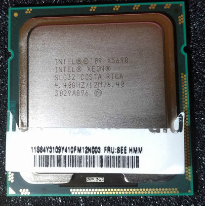
Xeon X5698 – Westmere – 4.4GHz – Mid 2010
The next well know Everest was a chip based on the Westmere (shrink of Nehalem) architecture. The Westmere Everest became known as the Xeon X5698, and was available for OEMs only, in fact it was a special order processor made with one particular type of client in mind. These were to be used for High Frequency Stock traders, and other such high speed transactional processing, where the ability to complete trades as fast, and reliability as possible is the entire nature of the business. This means that single thread performance is far more important then having multiple core, and as such, the X5698 uses a 6-core die with only 2 cores active, but retaining access to the entire 12MB of L3 cache. Clock speed was fixed at 4.4GHz, the cores did not reduce frequency as processing demands changed, as this would introduce uncertainty in how fast it would complete a given task. Doing task ‘X’ should take a predictable amount of time and not depend on what speed the processor chose to run at. The next fastest Westmere processor was the X5690, which was a 6-core (all cores enabled) running at 3.46GHz (the same chip essentially as the Core i7 990X). The X5698 was nearly 1GHz faster. The X5690 cost around $1800, where as the X5698 cost around $20,000 EACH (based on costs OEMs charged to add a 2nd one so they may have marked it up some). The impressive thing is that these chips would go faster. Intel sampled 4.66GHz versions and Supermicro built systems using X5698’s overclocked to 4.8GHz. All this back in 2011.
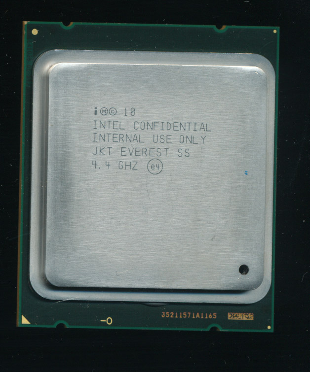
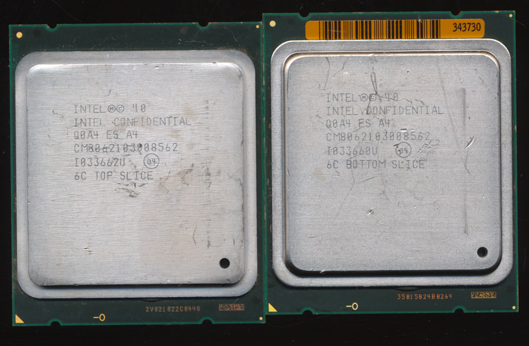
4.4GHz Jaketown (Sandy Bridge) Everest Sample 2010-2011
Intel’s next architecture was known as Sandy Bridge. Sandy Bridge topped at at 3.5GHz (6-cores) for the Core i7 Extreme 3970X and 3.6GHz for the 4-core i7-3820 and similar Xeon E5-1620. Intel demo’d an air cooled Sandy Bridge running on stage for a presentation at 4.9GHz, so the core certainly had some room to spare. There is no documentation (that I could find) that Intel actually released anything faster then 3.6GHz, at least that I could find, but evidence suggests that they at least were thinking about it. The picture is a Sandy Bridge Xeon in LGA2011 marked JKT EVEREST SS 4.4GHZ INTERNAL USE ONLY. JKT is short for Jaketown, Intel’s codename for the 32nm Xeon E5-2600 series. That gives a very good idea what this processor was to be. SS is likely to be a Single Socket (as often at those speeds getting dual systems working can be tricky). Sandy was certainly capable of hitting 4.4GHz, with 4-core, and even air cooling, so perhaps these were samples for a limited OEM run, much like the previous Westmere X5698 processors.
Tags:
everest, Intel, ivy bridge, Sandy Bridge
Posted in:
CPU of the Day