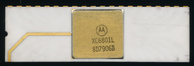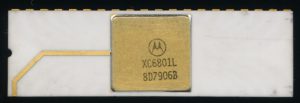
Motorola XC6801L – Early White ceramic package from early 1979. XC denotes a not fully qualified part.
A microcontroller (or microcomputer) is a CPU, with additional on-board peripherals, usually containing RAM, ROM, and I/O as to serve as a single (or close to single) chip solution for a computer system. As the program space is typically small, they were designed and used for high volume, low cost, simple applications. Today we would refer to them as embedded applications. The Motorola MC6800, released in 1974 was a decent 8-bit processor. It was however not inexpensive (a fact not lost upon one of its designers, Chuck Peddle, who left to design the 6502). Initial pricing for the MC6800 was $360, dropping to $175 the next year.
For embedded use, prices needs to be in the few dollars range, with as little chips as possible required for a design. By 1977 Motorola had a solution, the MC6802. This MC6802 was an enhanced MC6800 128-bytes of RAM and an on-board clock-generator. When combined with the MC6846 (which provided ROM, I/O and Timers) a complete system could be built. Defective MC6802s were often sold as RAM-less MC6808s.
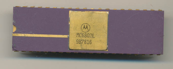
Motorola MC6802L – Dated March of 1978. The 6802 had 64-bytes of RAM and no ROM.
The MC6802 was followed by the more complex MC6801, which integrates the features of the MC6846 on die, making a true 8-bit single chip microcomputer. Most sources refer to the MC6801 being released in 1978, however it was actually released in 1977, likely at the same time, or similar as the MC6802. US Patent Application US4156867 filed on September 9th of 1977 references both processors. GM was to be the lead customer for the MC6801, it was the MCU of choice for the digital trip meter (TripMaster) of the 1978 Cadillac Seville. The 1978 Seville began production on September 29, 1977 on a 5.1um NMOS process. It is likely that all of the first production of the 6801 was reserved for GM, and it wasn’t until 1978 and later that Motorola began to market it (it begins to show up in Motorola marketing only in 1979). In 1979 the MC6801 also switched to a 3.9um HMOS process, which likely increased yields and decreased costs. The TripMaster was a $920 factory option that proved to be rather unpopular, likely due to it adding nearly $1000 in cost to a $14,000 car.
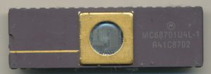
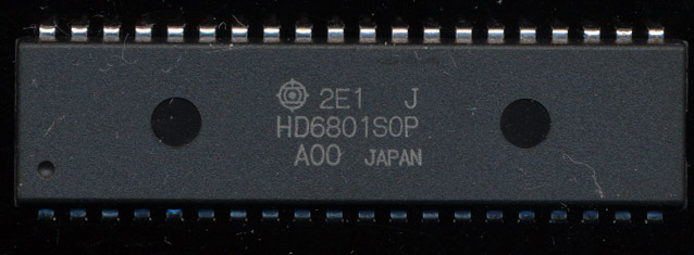
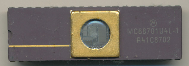
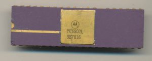
Motorola MC68701U4L-1 1987 6801 with upgraded RAM/ROM and Timers
This lack of early availability, coupled with the fact that while capable, the 35,000 transistor 6801 wasn’t particularly inexpensive led it to have very little success in the market. The EPROM version, the MC68701 infact is much more common, likely due to the fact that it was used in lower volume products, where cost wasn’t such an issue. In 1979 Motorola attempted to remedy this by releasing the MC6805 series. This was designed from the ground up to be low cost. The first versions had half the ROM and half the RAM as the 6801, while keeping the I/O. They were also available in CMOS (as the MC146805). They were inexpensive, and highly functional, and were widely used. The 6805 continues to see use today as the 68HC05 and 68HC08 series.
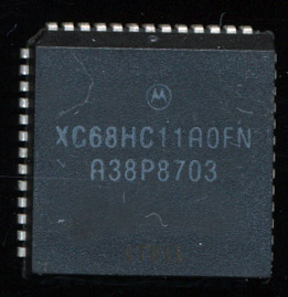
Motorola XC68HC11A0FN – 1987 – Preproduction, Enhanced 6801
The MC6801 was not, however, done. By this time manufacturing had improved, allowing costs to be lower. Motorola released an upgraded 6801, the MC6801U4 which expanded the timer functions, increased the ROM to 4K, and increased the RAM to 192-bytes. In 1985 the MC6801 was upgraded again, a second 16-bit index register was added, as well as true bit-manipulation instructions. The Motorola MC68HC11, the name change reflecting the greatly enhanced core, was made in many varieties with different sizes of RAM, ROM, and EEPROM. The MC68HC11A8 was also the first MCU to integrate EEPROM on die, in this case, 512 bytes worth. The MC68HC11 series, and its 68HC12 and 16 successors, continue to be made, and used today, ironically, frequently in automotive applications, where the original MC6801 failed to be a success.