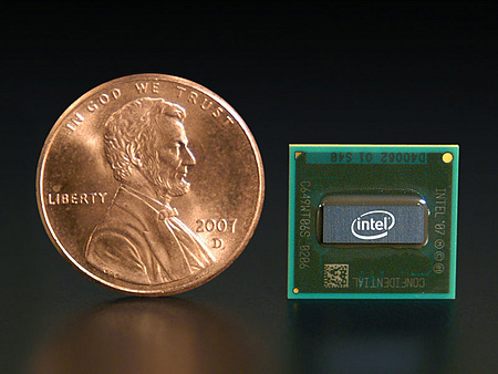
Anandtech and Chipworks deconstructed an Apple A8 processor, the hear of the new iPhone 6. By their analysis it is not a radical departure from the A7. It includes a slightly upgrade, but still quad-core, GPU, and an enhanced dual core ARM processor. The focus here is clearly on battery performance rather then sheer speed. Perhaps most interesting is the move from Samsung’s 28nm process to TSMC’s 20nm process (Being made by TSMC will hopefully put to rest the rumors of an Apple/Intel tie up once and for all.). This results in lower power, a smaller die area, and, assuming yields are on par, a lower cost per chip. Clock speed appears to be close to the same as the A7 at around 1.3GHz, with most performance improvements being architectural. It would appear to be the smallest improvement in the Apple A series, certainly since the A4->A5.
Considering the incremental improvement from the A7, one can only imagine what Apple has in mind for the A9 which is no doubt well under development.
It’s well known that Intel missed the jump on tablet and phone processors. Intel sold off their PXA line of ARM processors to Marvell in 2006, in an attempt to ‘get back to the basics.’ It turned out that this sale perhaps was a bit premature, as the basics ended up being mobile, and mobile is where Intel struggled (by mobile we mean phones/tablets, not laptops, which Intel has no problems with).
In January of 2011 Intel purchased the communications division of Infineon, gaining a line of application and baseband processors, based on ARM architecture of course. Intel developed this into the SoFIA applications processor, which was ironically fab’d by TSMC. Eventually the designs would be ported to Intel 14nm process, or that was the plan.
Intel Atom – Now by Rockchip?
So this weeks announcement that Intel has signed an agreement with the Chinese company Rockchip, to cooperate on mobile applications processors is a bit of a surprise, but the details show that it makes sense. Rockchips current offerings are ARM based, much as Intel’s current SoFIA processor, as well as Apple Ax series, Qualcomm’s SnapDragon, TI’s OMAP, etc. However, the agreement with Rockchip is not about ARM, its about x86. For the first time in many years Intel has granted another company an x86 license, specifically, Intel will help ROckchip build a quad-core Atom based x86 processor with integrated 3G modem. Rockchip currently uses TSMC as their fab, however also with this agreement Rockchip gets access to Intel 22nm and 14nm fab capacity.
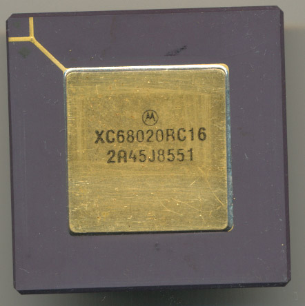
1985 production 68020 ‘XC’ denotes a not fully qualified device.
In 1979 Motorola wow’d the world with the introduction of the MC68000 MACSS (Motorola Advanced Computer System on Silicon). One of the first single chip 32-bit processors. In 1982 the design was upgraded and revised, and released as the 68010. Performance wasn’t that much better then the original 68k so it saw much smaller adoption.
In 1984 Motorola continued the 68k line with the 68020. Speed was greatly improved, up to 33MHz. It was originally made on a 2 micron HCMOS process, allowing the design to use 200,000 transistors and integrate additional addressing modes, co-processor support, and multi-processor support.
The Swedish Computer archeology blog Ehliar has a nice article and die shots on its architecture and design. Check it out.
Recently another antique computer was restored to working condition. Originally called the Harwell Dekatron, the WITCH (Wolverhampton Instrument for Teaching Computing from Harwell) was built in 1949-1951. Back in the early days of computing, it often took years to build a computer, rather then the minutes it takes to make a iPhone in today’s factories.
The WITCH was a decimal computer, storing data not in 0’s and 1’s of the transistor age, but actual decimal digits. It originally could store 20 8 digit numbers (0-99,999,999 or 23 binary bits) but later was upgraded to support up to 40, which was considered more then enough (such short sighted statements did not end in the 50’s, if you’ll remember Bill Gates comment about 640k of RAM is all anyone would need.) Data on the WITCH was stored on Dekatron tubes, a Cold-cathode device filled with Neon (or Argon) that could represent 10 digits. Sending a pulse to the Dekatron would cause the glowing Neon dot (and its associated high voltage) to move from cathode to cathode, thus allowing data to be stored. One side effect of having decimal data, and glowing orange dots for volatile storage is you can literally SEE what is in memory.
Dekatron in operation (courtesy of tube-tester.com)
The WITCH was mainly used to perform mathematical computations. It was not a fast computer, it took it a good 10-15 seconds to perform a multiplication. Many humans with adding machines could actually work the problems faster, however the WITCH never complained of carpal tunnel nor did it need breaks. The Harwell Dekatron was slow, but is was steady and quite reliable. It could go for days (providing it had enough problems fed to it on paper tape) without error or breakdown and that is what made it so useful and worth restoring.
Check out the BBC article and video of its operation and listen to the relays click, and see the glowing Neon of computational history.
Paul Allen, co-founder of Microsoft, has just opened the Living Computer Museum in Seattle. Living, of course, due to the fact that many of the vintage computers on display are working units. Some very rare systems including the only working PDP-7 in the entire world (UNIX was created to run on the PDP-7, so its a rather famous machine) and other DEC’s are on display. There are original IBMs, TRS-80s, Novas, and yes even some Apples. No Apple 1 as of yet. Perhaps Paul could pick up this latest one on auction? Should go cheap as it seems to be lacking an original MOS 6502 CPU.
The HP Input Output Blog has a nice write up on the floppy disk/drive. A very interesting read about a device many took for granted, and many of today’s generation did not ever get to experience. Many do not realize its humble beginnings, and the importance that Steve Jobs, ‘the bum in the lobby,’ played in the 5.25″ floppy becoming a standard. The 5.25″, holding twice what a 8″ floppy could, was developed by Shugart Associated in 1976. Shugart went on to become Seagate, known today for their hard drives. Hard drives that can store over 2 Terabytes of information. The original 5.25″ floppy? 160K, per side. An 8 inch? 80K a side. Interestingly enough, it was sometime before the Floppy Drive Controller (FDC) was integrated onto a single chip. Many original Shugarts used an Intel 8080 CPU for drive processing. The Commodore 64’s famous 1541 Floppy Drive ran its own 6502 type CPU, and was designed in such away you could actually load code directly to the floppy drive 6502. In the 1990’s attempts were made to increase the capacity, speed, and versatility of the floppy. Apple created a 2.88MB 3.5 inch floppy that never really caught on. There was the LS-120 drive which could use normal 1.44MB disks as well as special 120MB disks (was handy, but so few people had them, they had limited use). Ultimately, like most all technology the floppy has passed by the way side, today’s floppy is the USB Flash drive, holding many gigs of data for only a few dollars. And like the floppy, flash drives are used commonly for sneakernetting files around the office. Perhaps the mbile version of the floppy is the Micro-SD card, remember when Sony built a camera with a 1.44MB floppy drive built in? Not een large enough to store the picture from a cell phone camera today.
Yesterday Hans Camenzind passed away at the age of 78. Hans was a notable inventor of Swiss decent. Perhaps the most famous of all his inventions occurred in 1972 while working on a contract with Signetics he invented the 555 Timer chip, a simple oscillating IC that was inexpensive, and easy to build with. Now, even 40 years after its introduction, around a billion per year are still made, by dozens of companies around the world. The 555 Timer is often one of the very first IC’s electronics hobbyist begin experimenting with. Its applications are far reaching and while certainly not a CPU, its significance, and that of Camenzind, should not be forgotten.
The 555 Timer has of course been used in many many computers, notably in the Apple II computer as a joystick controller (558 Timer, which is a quad 555). Other uses include the IBM PC, Ataris, and many many more. In honor of Hans Camenzind, and the 555 Timer, go experiment with one and experience the joys of a device over 40 years old. Dont have one? They cost a whopping $0.95 at Sparkfun.
The Spacecraft CPU page has been updated, after a long gap. It now includes information of the recently landed Curiosity Lander, some new information on the 45 year old Voyager series as well as some on New Horizons, DAWN, and several others, so check it out.
Leaving on a trip so I dumped all the pending CPUs/EPROMs etc to a gallery.
There are litterally thousands of new CPU’s, EPROM’s, FPU’s, and some oddities.
They are sorted by manufacturer (technically brand)
Hard to imagine its been 30 years since IBM released the 5150 Personal Computer for the grand sum of $1265 thus starting the flood of PCs. Build with generic hardware, and MS-DOS from Bill Gates and crew (itself only released a month prior), the 5150 did away with proprietary, the MS-DOS OS was not exclusive to IBM, and the hardware was essentially off the shelf, using Intel’s 4.77MHz 8088 (cut down version of the 8086) processor and a discrete 256k of RAM. Other companies, could, and did, in mass, replicate and add to the 5150 making the 8088, and with it the x86 instruction set the de facto standard even to today. (though ARM has been making a large impact as of late due to the rise of mobile computing)
Here is an early add for the 5150, not only have we come a long ways in computers, but advertising as well.
In my daily hunt for new processors, and other chips for the museum, as well as information about new chips, I constantly come across interesting chips, in strange locations. Here you will get a chance to learn WHERE many of the chips in the museum come from and what they are.