
AMD Am29C327: How to Take a Picture of a Black Hole
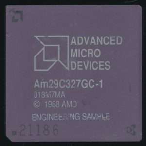
AMD AM29C327 Engineering Sample -1990
Recently I came across one of the more unusual members of the AMD Am29300 series. These were a set of processor elements (multipliers, FPUs, ALUS, registers) AMD designed to support AM29000 CPUs as well as for the bases for custom CPU designs. Some. like the AM29C323 multiplier found common use in video game and other applications. Others like the AM29C325 32-bit FPU were used in educational experiments and research. The 29300 (Bipolar) and 29C300 (CMOS) series are not particularly well known due to their obscure and often deeply specialized used. At the top of the series lies the AMD AM29C327 Double precision (64-bit) FPU. This FPU has a few tricks up its sleeves and is about as obscure in use as it gets….
The Am29C327 was on of the first chips made on AMDs CS-11A 1.2u processor (an enhancement of the 1.6u CS-11) . It was first announced in 1987 with sampling to begin in late 1988. The ‘327 contained over 250,000 transistors and was packed in a 169PGA package. It is a IEEE754 compliant double precision FPU but also supports IBM and DEC formats. It has 3 32-bit buses (2 for input and one for output) that, when multiplexed, allow for 64-bit maths. Its little brother, the ‘325, only supports 32-bit math, and comes in a 145PGA package with around 30,000 transistors (11,000 gates). So why does going to double precision involve nearly 10 times the transistor count? It turns out that the ‘327 is more closely related to an actual CPU then a normal FPU. The ‘325 has all of 8 instructions (add/sub, mult const subtraction and some conversions), while the ‘327 supports 58 instructions. Of those 58 instructions 35 are Floating point, 1 is system management, and the other 22? Those are a full set of integer instructions. The ‘327 actually supports more then just floating point. Its internal ALU is a 64-bit 3 input design, allowing inputs from either the 2 external inputs, the output, a set of 8 64-bit registers, or a set of 6 constants. Its instructions are 14 bits and it supports pipelining for even faster calculations. Interestingly, pipelining can be disabled and the FPU will work in straight flow through mode. So where is such a complicated chip used? Doing complicated math of course.
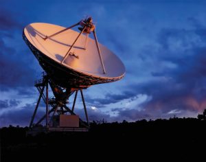
VLBA 25 Meter Antenna – NRAO
One such need for complicated math is in VLBI (Very-long-baseline interferometry). VLBI is using a series of radio telescopes or antennas, spaced apart physically, to generate higher resolution data then a single antenna could. The VLBA (Very-long-baseline array) is the largest of these, consisting of 10 25 meter radio telescopes spread across the USA. The maximum distance between them is over 5500 miles, so with the right software and hardware, working together, they can emulate a single dish of several thousand miles diameter. Production of this VLBA began in the late 1980’s and it went online in 1993. One of the hardest parts of running a VLBA is correlating the data, data from each telescope must be precisely combined to generate the resulting observable output. This is the job of the VLBA correlator, and as originally designed (and ran in such configuration at least into the 2000’s) this was based on a Motorola 68000 CPU driving multiple math cards. These math cards (mainly responsible for FFT – Fast Fourier Transforms) were
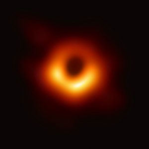
M87 Black Hole – Imaged by Event Horizon Radio Array in 2017
managed by a single Dallas DS87C520 MCS-51 MCU that set up the data for a pair of AMD AM29C327 FPUs and a Xilinx FPGA to process. A bit amazing that an 8-bit MCU was responsible for managing not one but two 64-bit FPUs, but in actuality all it had to do was route data to the proper places at the proper times, a gate keeper for the card.
Recently the VLBA, working together with other arrays to form the ‘Event Horizon,’ was able to take the very first ‘picture’ (radio data visualized) of an actual black hole. Today’s arrays typically use modern CPUs, or even super computers (the LOFAR uses an IBM Blue Gene/P) to perform their correlation, this results in data output much quicker then the sometimes days it took the original VLBA to process data. It all began with a 64-bit FPU from AMD in the 1980’s and scientists wanting to see what they could do.
December 20th, 2020 at 12:52 am
Wish I were following your blog earlier.. I just stumbled upon it today and these stories are fantastic.
I wrote a couple of trivial programs for the VLBA Correlator when I first arrived at the NRAO in 1998. I am still embarrassed at how long it took me to understand some very basic facts of interferometry. My toy program just spit out a couple of parameters for the control system that coordinated the Correlator and the 9-track tape drives that were used to feed the data from the antennas.
Twenty years ago, and I am still learning things!
November 6th, 2023 at 4:57 pm
I was one of the architects of the AM29C327 in the mid-80s and later wrote the User’s Manual. Amazing to see this fairly recent application of a chip that I thought had vanished into obscurity a very long time ago.
Thanks for the great blog!
Charlie