HP 3000 Series 33: 16-bits of Sapphire
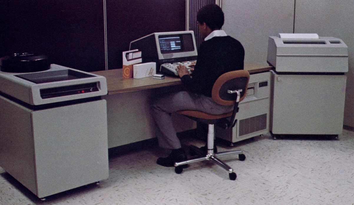
HP 3000 Series 33 – 16-bits 11MHz. They were integrated into the desk, with a 20MB hard drive on the left, and the computer on the right (with a 1.2MB 8″ Floppy Drive)
In 1972 HP introduced the HP 3000 line of minicomputers. Mini of course meaning they didn’t take up the entire room. They competed against the likes of the DEC PDP-11 and the TI-990. Original called the System/3000 (apparently to compare favorably to the IBM System/360) they were renamed the HP 3000. These were 16-bit computers employing a stack based design, They had no general purpose registers, all operations operated directly on one of several stacks. The first models were designed using bipolar discrete logic and ROM for the microcoding. This allowed for good performance but was expensive and large. Just the processor for the high end Series III of 1978 was 9 boards.
The Series 33 (and the smaller series 30) were to be cost reduced versions, to slot in between the high end Series III and the newly introduced HP 300 microcomputer. In order to do this those 9 boards for the processor needed to be greatly simplified. HP engineers decided to use a processor they had already, the CPU from the HP 300 Amigo. The HP Amigo was a bit of a disaster for HP, after 5 years of development, including
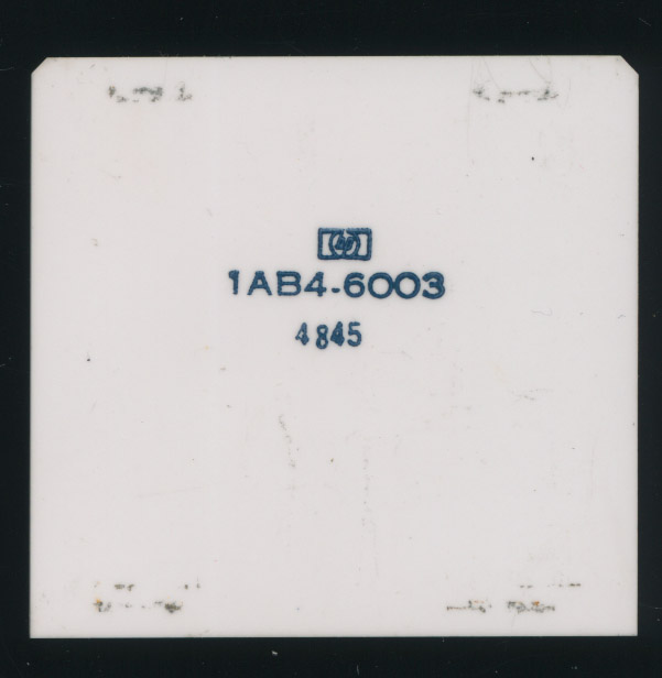
1AB4-6003 RALU -Silicon on Sapphire – 8000 Transistors
designing an entirely new processor it was a failure in the market, suffering from management and politics more then from a technical standpoint (it was not file system compatible with the 3000 line and that caused some concerns). After being released in 1978 it made only around $15 million in sales and was canceled after a short time.
Part of that 5 year development was for its 16-bit VLSI processor. In order to get the speed needed for the HP 300 and at a low price, the pressor needed to be a VLSI design (a few chips rather then a few boards). In order to fit in a smaller pedestal cabinet it needed to energy efficient and heat efficient as well. HP’s engineers decided to use a Silicon On Sapphire (SoS) CMOS design, a process HP had some great experience with in the MC2 processor. SoS is a form of Silicon on Insulator, a manufacturing method that is very common in today’s IC’s (using Silicon Dioxide). Instead of an IC being made on a pure silicon wafer, the silicon is deposited on a wafer of sapphire. Sapphire is an excellent insulator which wels reduce leakage currents, as well as spurious currents from such things as radiation. Radiation tolerance is perhaps what SoS became known for most, but its low power performance was what HP was after in the 1970’s.
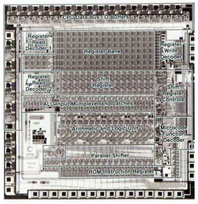
Die shot of the RALU with labels.
The processor for the HP 300 was designed into 3 separate IC’s, totaling 20,000 transistors (some documentation says 25,000) and running at a clock of 11MHz. The processor control unit (PCU 1AB2-6003) chip generates microinstruction addresses that control the other two chips: the register, address, skip, and special (RASS 1AB3-6003) chip and the register, arithmetic, and logic unit (RALU 1AB4-6003) chip.
The PCU contains 5000 transistors and handles the microsequencing, clock generation, and a sub-routine save stack. Clock generation is interesting as its single phase, and variable. The PCU can lengthen or shorten the clock period as needed. If a memory operation needs longer to complete the PCU simply holds the lock period longer. Data path functions are handled by the RASS and RALU chips. The RASS contains about 7000 transistors and contains a register file for the second operand to the RALU as well as address generation and skip logic. The largest of the chips is the RALU. It handles all of the standard ALU functions as well as hardware multiply/divide. It also contains 16 registers: 8 general purpose registers, and 8 for address storage. Together these three chips form the CPU of the HP 300 and consume only 1Watt of power. The processor is a microcoded design so the actually instruction set resides in ROM, in this case on a separate board. In the case of the HP 300 this also allowed the I/O processor duties to be microcoded into the general processor, eliminating another subsystem.
Posted in:
CPU of the Day