Archive for November, 2015

November 16th, 2015 ~ by admin

MHTL: Before the Processor

Motorola MHTL - Almost the entire product line is shown. Made from 1967-1972

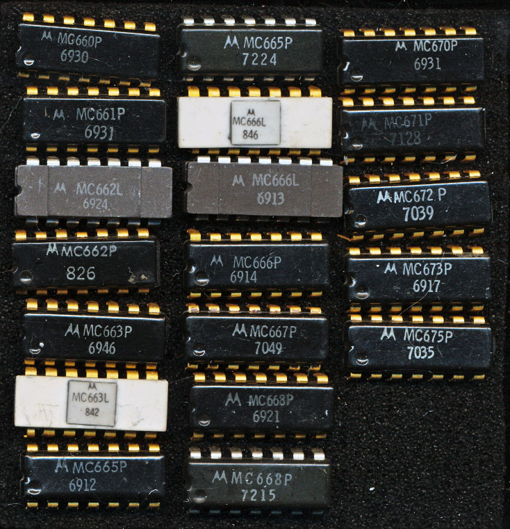
Motorola MHTL – Almost the entire product line is shown. Made from 1967-1972

Before the single chip processor, the Intel 4004, TI TMS1000, or Four Phase AL-1 (depending on your school of thought) ‘processing’ was done by discrete logic.  These are SSI IC’s (Small Scale Integration), a step up from literal discrete transistors, each IC contains 2-30 transistors, implementing a couple gates.

The most famous of these is the TTL (Transistor-Transistor Logic) series developed by Sylvania in 1963.  Before TTL though their was RTL (Resistor-Transistor Logic) in 1961 and the next year, DTL (Diode-Transistor Logic), whereby Diodes were added to the inputs, allowing much better fan-in.  Neither of these designs had great noise immunity, which in many applications was very important.  Motorola patented a modification to DTL in 1966 with production of the new MHTL family commencing in 1967-1968.

MHTL, Motorola High Threshold Logic, was designed for environments where high noise immunity was a must.  Noise, really any voltage that is present, and not wanted/not an actual signal, can be complicated to deal with.  Motorola’s solution was to make the signal much larger, this s clearly the ‘bigger hammer’ approach to noise.  Normal DTL has a turn on voltage of 1.5V (0-5V Logic). fairly low, and in an industrial environment, where these IC’s may be controlling large motors and solenoids, a common noise voltage.  MHTL raised that to 7.5V, requiring a 15V supply.  Speed suffers greatly, as the voltage must now swing from 0-15V for a logic 0 to a logic 1 on the outputs, 3MHz being a typical max compared to 40MHz for Motorola’s DTL.  It should be noted, that as fast as that sounds, it’s only for a few gates, a full board of these will not be able to attain anything close to 3MHz due to propagation delays through the many IC’s.

The pictured MHTL devices are:

Device Function Transistors Power (mW)
MC660 Exp 4 Input NAND (Passive Pullup) 6 88
MC661 Exp 4 Input NAND (Active Pullupt) 4 88
MC662 Expandable 4-Input NAND Line Driver 6 180
MC663 Dual J-K Flipflop 24 200
MC665 Triple Level Translator (for interface to DTL, RTL or TTL) ?? 104
MC666 Triple Level Translator ?? 105
MC667 Dual monostable multi vibrator ?? 240
MC668 Quad 2-Input NAND Gate (Passive pullup) 8 176
MC670 Triple 3-Input NAND Gate (Passive pullup) 6 132
MC671 Triple 3-Input NAND Gate (Active pullup) 9 132
MC672 Quad 2-Input NAND Gate (Active pullup) 12 176
MC673 Dual 2-Input AND-OR-INVERT (Active pullup) ?? 160
MC675 Dual Pulse Stretcher/Multivibrator ?? 180

Today, noise immunity is still relevant, and much much more complex than simply increasing the supply voltage.  Higher supply voltages not only slow down switching, but they also increase power draw significantly. The MC660 pictured has exactly 2 gates (4-input NAND), consisting of 6 transistors, and still dissipates 88mW. That would be the equivalent of an Intel 4004 dissipating 12 Watts, or an Intel 386 needing about 4 Kilowatts. Modern noise immunity is handled by adding additional transistors (keepers, pre-chargers, etc) that can keep gates from being affected by noise, whether it’s from power/ground lines, leakages, or other reasons.  This allows chips with millions of transistors to operate at sub 1 Volt levels.  An impressive feat.

Tags:
, , ,

Posted in:
CPU of the Day

November 8th, 2015 ~ by admin

Sun UltraSPARC IIIi+: The Serrano

Sun UltraSPARC IIIi+ Early engineering sample from August of 2005

Sun UltraSPARC IIIi+ Early engineering sample from August of 2005

In early 2004 Sun Microsystems had a lot going on.  The UltraSPARC IV had been announced, and Sun was already talking about its upgrade, the UltraSPARC IV+.  Sun had recently released the Jalapeno, aka the UltraSPARC IIIi, their second processor with on die L2 cache (The first being the IIe designed for embedded use) in 2003. In 2002 Sun had purchased Afara Websystems for their SPARC design, known as Niagara, which became the Sun T1, and were working on its successor, the T2.  Both the T1 and the UltraSPARC V (the successor to the not even itself yet released IV) was scheduled to tape out the next year, yet itself was canceled in April of 2004, most of the entire engineering staff working on it is laid off.

At the same time Sun was talking up an upgrade for the lower end UltraSPARC IIIi, this would be a relatively simple process, more the existing core to a new process.  It currently was being made by TI on a 130nm 7-layer Cu interconnect process with low-k dielectric.  Moving it to TI’s 90nm process would allow for greater clock speeds, less power, and room on die to quadruple the L2 cache to 4MB.  The processor was code named Serrano, and widely announced as an upgrade to Sun’s Fire V215, V245 and V445 servers. Sun promised a release in late 2005. And then…

Sun UltraSPARC III Cheetah - Early Mechanical Sampele.

Sun UltraSPARC III Cheetah – Early Mechanical Sample. The IIIi added on die L2 cache

Nothing, talk of the Serrano went silent, all PR focus has shifted to the coming T1 and the UltraSPARC IV+. Both are released in 2005 to great applause, but the tech community is still wondering where the IIIi+ has gone?  Sun isn’t exactly forthcoming as to why, mentioning that it had been delayed in order to get the T1 out the door.  In mid-2006 a customer commented, “There have been problems getting the UltraSPARC IIIi+ processors, so the new systems will be released with the current chips.”  Finally in August of 2006 Sun come forward and says that the IIIi+ has been canceled, but there is a catch, it was canceled the year before, and Sun decided to just keep mum about it.

Keep in mind the IIIi+, other then the increase in L2 cache, was a fairly ‘routine’ port to a new process.  The delays, and cancellation at the time sounded like it was due to technical grounds, but looking back, and seeing that they had working silicon in 2005, it would seem that the decision to kill the Serrano was resource driven.  Likely a combination of Sun’s engineering and marketing constraints, as well as the availability of the 90nm process at TI, which was also being used for the Niagara.

Manufacturing capacity is a finite resource, so not using up what may have been a very limited amount of fab space, on a processor that was designed to slot into the low end servers, is possibly the best explanation we have for the cancelling of the UltraSPARC IIIi+, perhaps a former Sun engineer can fill in some more details, as so many of them were laid off whom had worked on Sun’s previous processors.  It was a gamble by Sun, and one which seems to have paid off, considering the success of the Niagara, though Sun/Oracle were far from done with canceling designs, Honeybee, Rock, and M4 all come to mind.

Posted in:
CPU of the Day