Archive for October, 2015

October 20th, 2015 ~ by admin

CPU of the Day: Military Signetics 8X305 Processor

Signetics Military 8X305 - 1990 (8550201YA)

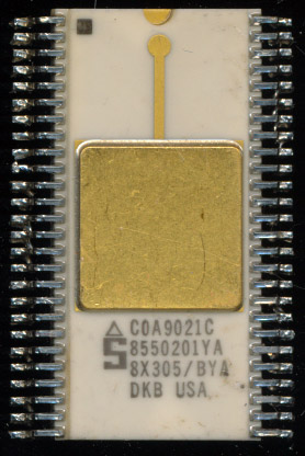
Signetics Military 8X305 – 1990 (8550201YA)

Some time ago we talked about the history of the Signetics 8X300 line of processors.  Originally released as the SMS300 in 1975 by SMS, the design was bought by Signetics.  It was a fairly unique 8-bit bipolar design, running at 8MHz. Its focus was signals processing, long before dedicated DSP’s such as the TI TMS320 came about.  The design was updated in 1982 to add some additional instructions and data handling.

Since it excelled so well at signals processing, the design worked well for military applications, where signals processing was of great use (interpreting data from a host of, usually, RF sensors.  The 8X305 was made in the normal 50 pin DIP, a 68 pin LCC, and an unusual 52 pin flat pack for military use.  In the 52-pin package the extra 2 pins are simply ‘No Connects’. (In the 68 pin version the extra 18 pins are divided amongst extra VCC, VR, GND, and N/C).

For military applications the greatest importance is on reliability.  This takes the form of three main areas:

Mechanical: How well can the design handle shocks, and vibrations, usually this is handled through better bonding wires, and more rigid package specs/inspection.
Electrical: How well can the device tolerate not great electrical conditions, higher reliability is achieved when the device can operate with a voltage that may very up to 10%, rather then the 5% or less commercial devices are designed to.
Temperature:  This is closely related to mechanical, as temperature stability requires the package to be damaged by expansion/contraction in wild temperature swings.  Obviously the silicon die itself needs to work with the same electrical characteristics at different ends of the temp range.  Many electrical parameters (such as resistance, and biasing) change over temperature, so the device must handle this. Typical military spec is -55C-125C (-67F-257F).  A range of 180C, from well below freezing, to well above boiling.

Venus - From the Mariner 10 Probe

Venus – From the Mariner 10 Probe

This Signetics 8X305 (Drawing # 8550201YA) is rated at -55-125C at 5V +/- 10% running at 8MHz.  It meets all the mechanical/inspection and testing requirements of MIL-STD-883 Class B.  This type of design work is well understood, and now a days, rather routine.  Making electronics work at 125C is no longer an engineering feat.  But then, what if we need more? Lots more.

Recently NASA contracted with Ozark Integrated Circuits to do just that.  NASA wants a process kit for IC’s that will run happily at 500C (932F) . At this temperature lead and tin have melted, and aluminum isn’t even very solid. If that sounds a bit inhospitable, you’d be right, and its exactly the conditions NASA faces with designing a rover for use on our nearest neighbor, Venus.

Ozark previously created such a process good for up to 350C, but thats still not hot enough for Venus.  Ozark is using a silicon carbide substrate, and some other proprietary methods.  They will not actually produce the chips for NASA, but rather licenses the methods to do so to a foundry service of NASA’s choosing, who will then manufacture and test them.

Surface of Venus, from Venera-13

Surface of Venus, from Venera-13

In the upper atmosphere, temps are below 0, and at the surface, atmospheric pressure is 90 times greater than on earth, another challenge for making a chip, with a die recessed in a sealed cavity.  Such requirements, and the technology to meet it, will greatly enhance our exploration abilities, and no doubt, trickle down in some way, to the electronics we use each day.

Posted in:
CPU of the Day

October 8th, 2015 ~ by admin

AMD 20 Processor Test Board – A Gang of Athlons

AMD Socket A Test Board

AMD Socket A Test Board

Processors are tested at many steps in the manufacturing process.  Automated visual inspections are done at several steps during the wafer lithography stage, the individual chips are tested and marked on the wafer before slicing, and then final testing and speed grading during the assembly process.

This board is part of that final test stage,  It is designed to test Socket A (462) CPU’s, 20 at a time.  The board was made by a company called DynaVision in June of 2000, coinciding with the release of AMD’s first Socket A processors.  The board would be used in a test machine, and likely manually loaded with up to 20 processors.  This cannot be a FULL test of the processor as not all signals are brought out (so it may miss a package defect).  All the test, debug and JTAG signals are brought out from each socket, as well as the necessary voltages and CLK signals provided.

A connector by each socket supports, PS_ON, PWERON, ANODE and CATHODE signals, though I am not entirely sure what there are for.  Best guess is thermal management.  Also next to this is 2 signals labeled TEC1 and TEC2, naming that may suggest Peltier junction cooling.

AMD 20 socket test board, circa 2000

AMD 20 socket test board, circa 2000

The board is labeled AMD 317-S6300 and FAB 30-21041B.  Fab 30 could suggest AMD’s Dresden Germany Fab, which would make this board even more interesting, as only a very few processors were assembled/tested at the fabs themselves.  Most production AMD processors were assembled and tested in Penang, Malaysia (since 1972).

Someone at AMD was certainly intimately familiar with the design and use of this board, and its part in AMD’s success in the market.  Now it occupies a few square feet of a wall at the CPU Shack Museum keeping its secrets to itself.

Tags:
,

Posted in:
Boards and Systems

October 1st, 2015 ~ by admin

Western Digital and the COP

Western Digital WD4200F-03 - Copy of National COP420

Western Digital WD4200F-03 – Copy of National COP420 from 1981

In the 1970’s second sourcing was the name of the game.  Processors that had no additional source available often struggled in the market.  Designers wanted to ensure that if they invested in designing a product around a chip, that chip would remain available if the original manufacturer of it had issues.  It also helped drive down pricing, as often second sources could compete on price with the original manufacturer.

By the 1980’s second sourcing had begun to end.  It did still happen, but began to take the form of fabless semiconductor companies today.  A company would create a design and then license its manufacturing to other companies.

National Semiconductor COP420 - 1982

National Semiconductor COP420 – 1982

National Semiconductor was a popular second source for many processors of the 1970’s, notably Intel’s 8080, MCS-48 microcontrollers and AMD’s 2901.  For their own designs, they rarely second sourced to anyone.  Such designs as the PACE, SC/MP, original COPS and NSC800 were exclusive to National.  In the 1980’s they did have TI make a very limited amount of 32k processors, likely due to some of the reliability problems National was having in making them themselves early on.  So it is a bit surprising that they licensed the COPS II to Western Digital in the early 1980’s.

Western Digital WD4210BG-15 - Bond out option of the WD4200

Western Digital WD4210BG-15 – Bond out option of the WD4200

The COPS II (later just called COPS) was the 2nd generation COPS 4-bit microcomputer made by National.  It was a NMOS design, designed for basic control oriented applications to replace the PMOS COPs from 1976.  Western Digital already had the 4-bit CR1872 PMOS processor, as well as the CP1611 16-bit design.  Perhaps WD saw the COPS as a filler between those.  It certainly didn’t replace the CR1872, as that design continued to be marketed up until the mid-1980’s.

Western Digital made the WD4200 and WD4210 as copies of the National COP420 and COP421.  Also made was a WD4020 copy of the COP402 (the ROMLESS version used for dev work).  The WD4200 and WD4210 are nearly identical to each other.  The 4200 comes in a 28-pin package while the 4210 came in a 24-pin package.  WD (and National) called this a bond-out option.  The die is the same in both, the 4210 merely has one 4-bit input port left unconnected (IN0-IN3).  A 24-pin package was enough less expensive than a 28-pin package to make this a viable sales option.  Using a bulk NMOS process the die itself was a fairly insignificant cost compared to packaging and testing. The smaller package also was useful for smaller board designs.  The practice continues today with features on processors and MCU’s disabled/enabled to expand a product line and/or make use of die’s with defects.

WD continued to produce the COP line until at least 1983.  Western Digital was moving its focus to the storage market, and away from te general purpose processor/microcomputer market.  This brought an end to the WD4200 as well as WD’s other processors.   Today WD is known for hard drives, and remembered for their disk controllers. that they second sourced a 4-bit design from National has faded to the annuls of history.