The 16-bit Transistor level MegaProcessor
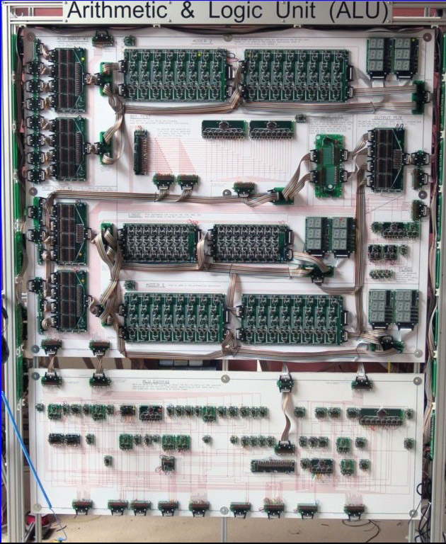
16-bit MegaProcessor ALU
James Newman in Cambridge (UK) is creating a 16-bit discrete Processor Design called the Megaprocessor (there is nothing micro about it). Not a VLSI version either, a 16-bit processor built of discrete transistors, hand wired, hand soldered, with debugging provided by…3500 LEDs. He admits perhaps things got a bit out of hand when a co-worker remarked that it would be helpful if a signal had an LED on it, thus providing the motivation to go out and build a complete 16-bit processor.
James estimates that the design (he is still building it) will take 14,000 discrete transistors, 3,500 of which are actually to drive the LEDs. ROM and RAM (256 bytes each, assuming he doesn’t get carpal tunnel from soldering it all) will be an extra 16,000+.
An original Intel 8086 used 29,000 transistors, and was a similar 8/16 bit architecture. The Novix NC4016 stack processor, also 16-bits, was a very clean design using only 16,000 transistors. HPs original BPC 16-bit processor from 1975 was 6,000, so James design is certainly inline with expectations (though his sanity maybe in question).
While this seems like a crazy amount of work (it is), This is how the first transistor computers were made. The original DEC PDP-1 from 1959, used 2,700 discrete transistors, and was an 18-bit design. The Apollo Guidance computer from 1966 was a 16-bit design (using IC’s with 3 transistors each, so a bit easier construction) used 12,300.
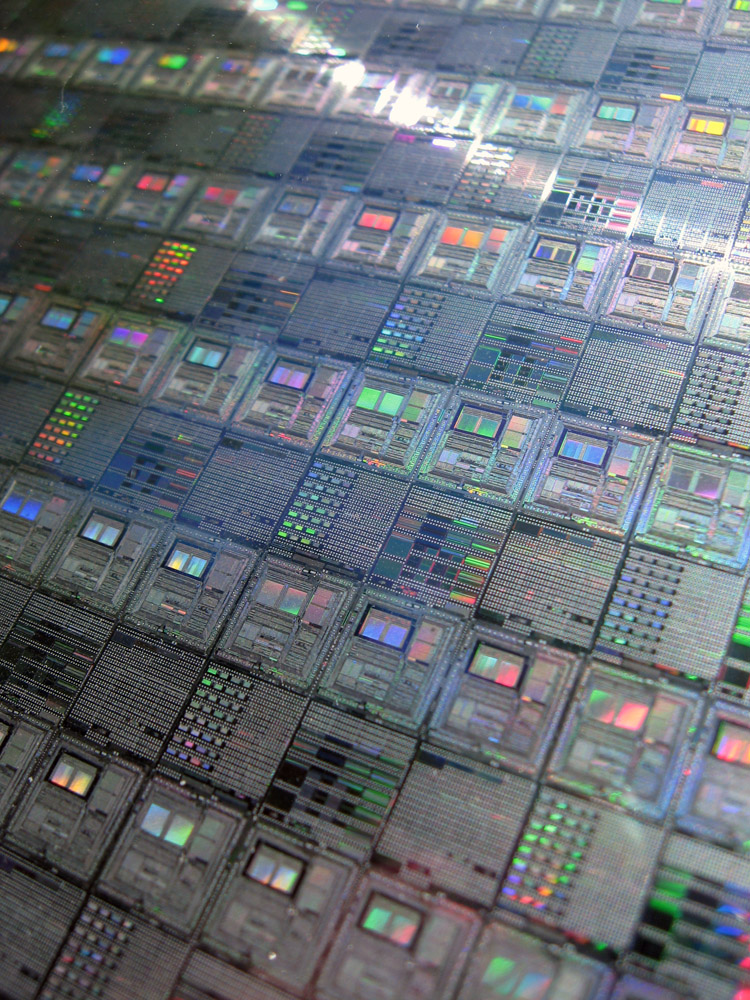
So while James’ design may be a bit over the top, it provides a good look back at where we have come. Today chips can have well over a billion transistors on a die smaller then a fingernail.
Posted in:
Just For Fun