February 27th, 2014 ~ by admin
Bloomberg Business Week recently published an interesting article on ARM’s rise to power in the processing world. There first major design ‘win’ was a failed product known as the Apple Newton, yet they would go on to become a powerhouse that is no challenging Intel.
In ARM’s formative years, the 1990’s, the most popular RISC processor was the MIPS architecture, which powered high end computers by SGI, while Intel made super computers (the Paragon) based on another RISC design, the i860. Now, nearly 2 decades later, after Intel abandoned their foray into the ARM architecture (StrongARM and X-Scale) RISC is again challenging Intel in the server market, this time, led by ARM.
MIPS, now owned by Imagination, is again turning out new IP cores to compete with ARM, and other embedded cores. Their Warrior class processors are already providing 64-bit embedded processing power, though with a lot less press that the likes of Apple’s A7.
February 18th, 2014 ~ by admin
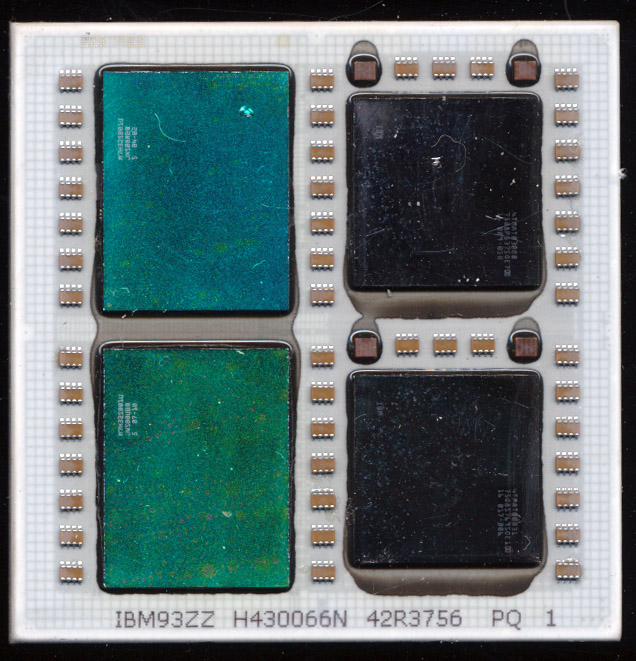
IBM POWER5+ QCM – 4 dies, 8 cores, and 72MB of L3 Cache
When the POWER5 processor was released in 2004 it was made in two versions, a DCM (Dual Chip Module) containing a POWER5 die and its 36MB L3 cache die, as well as a MCM containing 4 POWER5 die and 4 L3 cache dies totaling 144MB. The POWER5 is a dual core processor, thus the DCM was a dual core, and the MCM an 8 core processor. The POWER5 contains 276 million transistors and was made on a 130nm CMOS9S process.
In 2005 IBM shrank the POWER5 onto a 90nm CMOS10S manufacturing process resulting in the POWER5+. This allowed speeds to increase to 2.3GHz from the previous max of 1.9GHz. The main benefit from the process shrink was less power draw, and thus less heat. This allowed IBM to make the POWER5+ in a QCM (Quad Chip Module) as well as the previous form factors. The QCM ran at up to 1.8GHz and contained a pair of POWER5+ dies and 72MB of L3 Cache.
The POWER5+ was more then a die shrink, IBM reworked much of the POWER5 to improve performance, adding new floating point instructions, doubling the TLB size, improved SMP support, and an enhanced memory controller to mention just a few.
The result? A much improved processor and a very fine looking QCM.
February 9th, 2014 ~ by admin
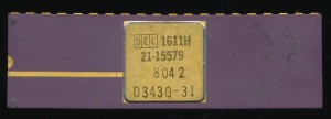
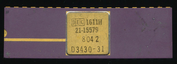
DEC 1611H 21-15579 – LSI-11 RALU (MCP-1600)
Fully 10 years before Western Digital released their first hard drive, they made processors, calculator chips, Floppy Disk controllers and a host of other IC’s. Western Digital began in 1970 making primarily calculator chips. In 1976 they announced the multi-chip MCP-1600 processor. This was an implementation of the PDP-11 minicomputer in silicon. It consisted of a CP1611 Register/ALU chip, a CP1621 control chip and either 2 or 4 CP1631 512x 22bit MICROMs that contained the microcode implementation of the PDP-11 architecture. Physically this was an 8-bit design, but clever microcode programming allowed it to function as a 16-bit processor. Use of microcode allowed it to also implement floating point support, a very new concept in hardware in 1976. The MCP-1600 was used in DECs LSI-11 microcomputer among others.
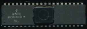
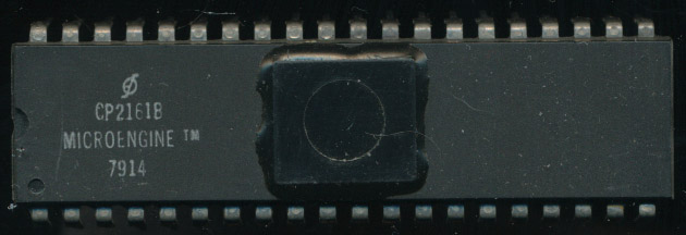
Western Digital CP2161B – 1979 Pascal Control Chip
Having the microcode separate from the ALU/Control didn’t help with board layout or cost, but it did provide a very flexible platform to implement other architectures on. In the late 1970s UCSD (University of California in San Diego) was working on a project, led by Kenneth Bowles, to make a portable version of the Pascal programming language, a version that could run on multiple hardware platforms, very similar to how Java has become today. The code was compiled to a ‘p-code’ or pseudo code that could them be executed by a virtual machine onto whatever hardware. Typically this virtual machine would be implemented in software, however the design of the MCP-1600 was such that it could be implemented in hardware, or rather microcode. Thus in 1978, the WDC MICROENGINE was born. This was to be a 5 chip set (original documentation states 4, but it ended up being 5) that consisted of the CP2151 Data chip (if you have a CP2151 you would like to donate, let us know) , the CP2161 Control chip, and 3 512 x 22 bit MICROMs which contained the microcode to directly execute UCSD Pascal on the data chip. The CP2151 was no different from the CP1611 of the MCP-1600 chipset and could be interchanged.
Read More »