December 6th, 2012 ~ by admin
 Over two years ago we wrote about the history of the Signetics 8X300 processor. A design that was one of the first DSP like architectures. The 8X300 was a design of the Scientific Micro Systems Inc. SMS300. You can read the entire history here.
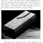
The only SMS300 I had ever seen was a picture of one in the 1976 issue of Microcomputer Digest (as seen here). Its a very unusual package, with very long leads. Recently I found one hiding in a scrap lot on eBay, and could nearly not contain my excitement when the seller confirmed its markings. Of course I purchased the scrap lot, and waited like a child before Christmas for it to arrive. When it did, I was happily surprised to find it intact, and in good condition (a relatively rare occurrence for a DIP in a scrap lot, especially a 36 year old one.

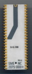
SMS 300 – Early 1976
Here you can see an original SMS300 dating from 1976. Interestingly enough the Signetics version is in a 50 pin package while the SMS is in a 48pin. I assume Signetics changed some of the power supply requirements for it but do not know for sure.

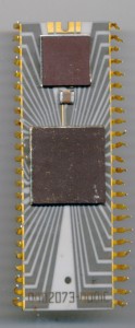
Back side showing stunning traces and die caps
Looking at the back of the processor you can see 2 large ceramic ‘caps’, one is for the die, the other appears to be a power circuit of some sort. These are over 2mm thick, which is one of the reasons for the very long pins. (8 mm long). If you have any additional info on the SMS300 (a datasheet perhaps) please let me know.
December 3rd, 2012 ~ by admin

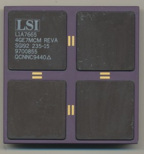
SGI Extreme 4GE7MCM 256 MFLOPS 320,000 Gates
At 2.6oz (75 grams) and 2.25 inches square (6cm) the SGI 4GE7MCM is a beast of a graphics chip. More properly called a Geometry Engine was, the GE7 was responsible for all the graphics processing in SGI Indigo2 workstations. The Indigo2 Extreme graphics option consisted of a pair of these MCMs (Multi-Chip-Module). Each one contains 4 GE7 Geometry Engines providing 32MFLOPS of performance each. Each GE7 consists of a custom 80,000 gate array from LSI (for a total of 320,000 gates and 128MFLOPS per MCM). This performance level was, ironically, better then the main system CPU (35MFLOPs for the 200MHz R4400 option).
Each of the black ‘caps’ on the chip covers a single GE7 Engine. A similar design was used for the XZ Graphics system that had only 4 total GE7 cores. This was either implemented with 2 of the large MCMs that had only 2 GE7s in them (same package however) that were marked 2GE7MCM, or, later, a single surface mount MCM containing 4 GE7 engines. All were manufactured by LSI. In total the Extreme Graphics subsystem had no less then 31 custom gate arrays from LSI for a total of over 1.2 million gates. At an average of 2 transistors per gate that works out to around 2.5 million transistors, a considerable amount for a graphics system in 1993. Today’s graphics chips pack in transistors numbering in the billions, the Geforce GTX 680 has a total of 3.54 billion transistors, and performance measured in TFLOPS, again for the GTX 680, 3.09TFLOPS. Today’s graphics chips cannot, however, compete with the magnificent looks of the GE7’s giant MCM package.
Sources:
Indigo2 Product Guide (PDF)
Indigo2 Technical Report
 Over two years ago we wrote about the history of the Signetics 8X300 processor. A design that was one of the first DSP like architectures. The 8X300 was a design of the Scientific Micro Systems Inc. SMS300. You can read the entire history here.

