Archive for October, 2012

October 31st, 2012 ~ by admin

Cyrix Joshua Processor – From Peppers to the Bible

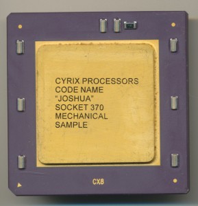
Cyrix Joshua Sample

Perhaps one of the most confusing, and misreported processor stories is that of the Cyrix Joshua processor.  More correctly known as the VIA Cyrix III Joshua.  Cyrix began sampling this successor to the MII in 1999, a tumultuous time in Cyrix’s history, as they were in the midst of being sold to VIA by National Semiconductor.  The Joshua never made it into full production, being quickly killed off by the Centaur designed Samuel core. Centaur was the processor division of IDT which produced the Winchip series, bought by VIA only a month after their purchase of Cyrix.

Adding to the confusion was Cyrix bountiful use of code names for its upcoming products, with many seeming to overlap, change or be redundant.  Understanding the methodology of their naming will greatly increase ones understanding of the products.  Cyrix used a code name for the core of a processor, as well as a separate name for what application that core was going to be used in.  Just like Intel used the P6 core for the PII, Celeron, and Xeon, Cyrix intended its cores to be able to be used in several products.

In the late 1990’s Cyrix had two new cores under development.  The first was the Cayenne, an evolution of the 6x86MX/MII processor.  The Cayenne was essentially an MII, with a dual (rather then single) issue FPU, support for 3DNow! instructions, and perhaps most importantly, a 256K 8-way associative on-die L2 cache.  It retained the 7 stage pipeline of the MII, the 256 byte scratch pad L0 cache, an almost identical X-Y integer unit and the same 64K L1 cache.  Cyrix had had industry leading integer performance, but always lagged in the area of FPU performance.  The dual issue FPU was their attempt to help remedy this.  However, FPU intensive benchmarks, such as Quake 3, showed the Cayenne core to be about half as fast as a Celeron of equal rating (500MHz vs PR500 Cyrix).  Business apps, heavy in integer and light on floating point, showed the integer strength of the Cyrix, with a 400MHz Cyrix matching a 500MHz Celeron.

The Cayenne core was slated to be used in at least 3 different products.  The first was the MXi, this was the successor to the MediaGX and thus would be highly integrated, including a PCI Bus controller, SDRAM controller, MPEG/DVD acceleration, 2D/3D Graphics as well as audio capabilities. The Jedi was to be a socket 7 (Super 7 really) compatible processor based on the Cayenne core.  This was canceled in 1999 (nothing to do with potential lawsuits from Lucas Films as often was rumored).  The third use of the Cayenne core was the Gobi, this was to be a Socket 370 compatible processor and it is this version that was widely sampled, and benchmarked, by many hardware review sites, magazines, etc.  When VIA purchased Cyrix on June 30, 1999 the Gobi project was allowed to continue, MXi, and other projects were quickly shut down.  The Gobi codename did not fit with VIAs core naming scheme however, thus is was renamed.

Read More »

Tags:
, , ,

Posted in:
CPU of the Day

October 26th, 2012 ~ by admin

Paul Allen’s Living Computer Museum Opens To Public In Seattle

Paul Allen, co-founder of Microsoft, has just opened the Living Computer Museum in Seattle.  Living, of course, due to the fact that many of the vintage computers on display are working units.  Some very rare systems including the only working PDP-7 in the entire world (UNIX was created to run on the PDP-7, so its a rather famous machine) and other DEC’s are on display.  There are original IBMs, TRS-80s, Novas, and yes even some Apples.  No Apple 1 as of yet.  Perhaps Paul could pick up this latest one on auction? Should go cheap as it seems to be lacking an original MOS 6502 CPU.

Posted in:
Museum News

October 16th, 2012 ~ by admin

Renesas: The Auto Bailout of the Semiconductor Industry

In 2003 Renesas Technology was formed as a joint company between Hitachi and Mitsubishi, combining their semiconductor operations.  In 2010 Renesas Electronics was created by the merger of NEC Electronics, and Renesas Technology.  This created the largest supplier of microcontrollers in the world, combining the product portfolios of NEC, Mitsubishi and Hitachi.  This allowed them to stop competing amongst themselves, and compete with Samsung, Infineon and other suppliers.

Renesas ended up with the following microcontroller families:

  • Hitachi: H8, H8S, H8SX, SuperH
  • Mitsubishi: M16, M32, R32, 720, 740
  • NEC: V850, 78K

In addition Renesas has developed it’s own designs including:

  • RX Series – a replacement for the Hitachi H8SX and Mitsubishi R32C designs.
  • RL78 Series – a replacement that combines the NEC 78k and Mitsubishi R8C devices
  • RH850 Series – successor to the NEC V850 for automotive use
  • R8C Series – Value derivative of the Mitsubishi M16C

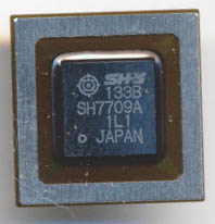
Hitachi SH-3

One of the largest markets for these microcontrollers (and associated other parts) is the automotive industry, with today’s vehicles containing, on average, $350 in just IC’s per car.  $350 may not sound like much when a car costs $20,000, but the Average Sale Price (ASP) per component, is 33 cents, meaning there are, on average, over 1000 IC’s in a modern car, of which 50-100 are microcontrollers.  They do everything from run the stereo, to monitor and adjust engine parameters.  As more features (entertainment, navigation, stability control, etc) are added, the count goes up.

The market downturn in 2008-2009 hit the automotive industry, and is suppliers very hard.  With very small profit margins this hit Renesas very hard as well.  Combined with increasing competition from Samsung  Renesas has been driven into high levels of debt, and a distinct lack of profitability.

Read More »

October 8th, 2012 ~ by admin

Apple A6 vs Rockchip RK3066: 4 Years vs. 6 weeks of design

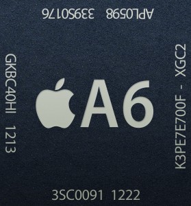
The introduction of the iPhone 5 was also the introduction of Apple’s first truly original Application Processor design.  The iPhone 2, 3G and 3GS all featured designs by Samsung.  The iPhone 4 introduced the A4, which was closely based on the Hummingbird Cortex-A8 core developed with Samsung and Intrinsity, again, not a truly Apple design.  The iPhone 4S introduced the A5 (and the A5X used in the iPad 2).  The A5 is based on the ARM Cortex-A9 MPCore, a standard ARM design, albeit with many added features, but architecturally, the processor is not original, just customized.

ARM provides cores designs for use by developers, such as the Cortex-A9, A8, etc.  These are complete designs of processors that you can drop into your system design as a block, add your own functions, such as a graphics system, audio processing, image handling, radio control, etc and you have your processor.  This is the way many processor vendors go about things.  They do not have to spend the time and effort to design a processor core, just pick one that meets their needs (power budget, speed, die area) and add any peripherals   Many of these peripherals are also licensed as Intellectual Property (IP) blocks making building a processor in some ways similar to construction with Legos.  This is not to say that this is easy, or the wrong way to go about things, it is in fact the only way to get a design to market in a matter of weeks, rather then years.  It allows for a wide product portfolio that can meet many customers needs.  The blocks are often offered for a specific process, so not only can you purchase a license to a Cortex-A9 MPCore, you can purchase one that is hardware ready for a TSMC 32nm High-k Metal Gate process, or a 28nm Global Foundries process.  This greatly reduces the amount of work needed to make a design work with a chosen process. This is what ARM calls the Processor Foundry Program.

Read More »

Tags:
, ,

Posted in:
Research

October 5th, 2012 ~ by admin

CPU of the Day: Fairchild F9450 – Commercial Military

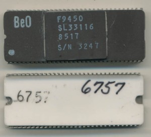
Fairchild F9450 – 1985 – 10MHz

In 1980 the United States Air Force published a standard for a 16-bit Instruction Set Architecture (ISA) to meet their needs for computers on fighters etc.  This standard is known as MIL-STD-1750A and laid out what the processor needed to be able to do, but not how, or what would be used to accomplish it.  This allowed manufacturers to implement the standard in anyway they wanted.  It could be done in CMOS, Bipolar, SoS, GaAs or even ECL.  It was designed (like the Signetics 8X300 and the Ferranti F100) with real time processing in mind, similar to what we would call a DSP today.

Many companies made 1750A compatible processors including Honeywell, Performance Semiconductor (now Pyramid), Bendix (Allied), Fairchild, McDonnell Douglas, and others.  The processors ended up finding uses in many things outside of the USAF, including many satellites and spacecraft including the Mars Global Surveyor.  The standard was not restricted to military use, in fact commercializing it was encouraged, as this would increase production, which would help decrease costs for the military.

Fairchild designed the F9450 to meet both the commercial, and military markets.  Initial availability was in 1985 and the F9450 provides an on-board floating point unit, an optional, second chip, on other implementations.  Fairchild also made a F9451 MMU (Memory Management Unit), and a F9452 BPU (Block Protection Unit).  The 9450 was manufactured in a bipolar process (Fairchild called it I3L for Isoplanar Integrated Injection Logic).  This helped boost speed, as well as greatly increased reliability, as bipolar is much less susceptible to higher radiation levels then CMOS is.  Bipolar processes also generate heat, lots of it and to help counter this Fairchild used a somewhat unusual (for a processor) ceramic package made of Beryllium Oxide (BeO).  BeO has a higher thermal conductivity than any other non-metal except diamond, and actually exceeds that of some metals. Normally the ceramic on a CPU package is some form of Alumina (Al2O3).  Beryllium itself is a carcinogen so grinding, or acid application on BeO is not recommended.  The bottom of the the 9450 was made with a different ceramic, as the goal was to get the heat away from the chip, and not back into the PCB.  9450s were available in speeds of 10, 15 and 20MHz and in Commercial, or Military temperature rating.  MIL-STD-883 screening was of course available.

By 1996 the 1750A architecture was declared inactive and not recommended for new designs.  However, due to its extensive software support, reliability, and familiarity, it enjoys continued use, and is still being manufactured by several companies.