Archive for March, 2011

March 31st, 2011 ~ by admin

CPU of the Day: MMI 6701 Bit-Slice

In 1974 Monolithic Memories Inc. (MMI) announced the 6701 bit slice device.  At its heart the 6701 is a 4-bit ALU much like the 74181 TTL IC.  The 6701 adds a register, and some other support circuitry on chip making it much more adaptable.  The 6701 has an approximate complexity of 1000 gates (meaning it would replace 1000 gates worth of TTL).  The 6701 was made on a bipolar process and ran at 5.2MHz.  Later versions would up this speed to around 11MHz.

6701D - 1976

The 6701 continues on until around 1980 by which time the AMD 2901 bit-slice processor had come to completely dominate the market.  The Soviets however cloned/modified the 6701 as the 1802VS1 through the 80’s and into the 1990’s.

Posted in:
CPU of the Day

March 17th, 2011 ~ by admin

Chips of the day: TI TMS320E The tale of the two dies

Its fairly common for a manufacturer to make several devices out of a single actual die.  Just disable part of the die, whether because its faulty, or not needed, or simply do not connect the pins to that feature.  Intel did this a lot with the Celeron, and PIII line, disable some L2 cache on a PIII and you get a Celeron.  Today it is done with multi-core processors.

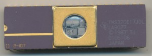
TI TMS320E17JDL

Using a common wafer for several products saves a large amount of money, no need for a second mask set, and testing systems.  Here we have a Texas Instruments TMS320E17JDL.  The TMS320 is the industry standard in DSPs (Digital Signal Processors). The E17  from 1990 runs at 20.5MHz has a 4K EPROM, 256 bytes of RAM, and a pair of serial ports.  You can see the large sections of the die devoted to the ROM, RAM, and MAC (Multiply and Accumulate).

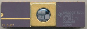
TI TMS320E15JDL

This is the TI TMS320E15JDL.  It is the same basic DSP core as the E17, it includes the same 4K EPROM, the same 256 bytes of RAM and the same MAC unit.  It has some I/O ports tasked with doing different things, but thats a relatively minor difference.  The big difference is the E15 lacks the 2 serial ports of the E17.  You can see on the die where that hardware does not exist, its a large black spot, void of any circuitry.  A very interesting and unusual occurrence.

TI either used a completely different mask for the E15, or they simply chose to not expose that small part of the mask.

Tags:
,

Posted in:
CPU of the Day

March 12th, 2011 ~ by admin

Apple A5 Updated Info

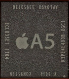
Now the UBM Techinsights and iFixIt have completed their teardowns of the iPad 2, and benchmarks have been run we now know that the A5 is in fact a dual core, made by Samsung, and clocked at around 900MHz.  It also includes the PowerVR 543 dual core GPU as we suspected in our previous post.

Apple A5 Processor

Also we now have an actual image of the chip, rather then the photoshopped one Apple used in their presentation.

Tags:
,

Posted in:
Processor News

March 6th, 2011 ~ by admin

CPU of the Day: NS87P50R-6: Piggyback CPUs

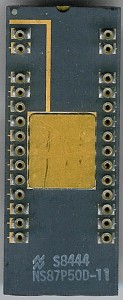
National Semiconductor NS87P50D-11
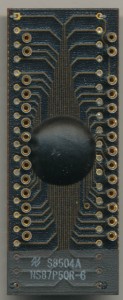
National Semiconductor NS87P50R-6

In the 1980’s most high-volume microcontrollers were OTP (one-time-programmable) or were factory programmed (Mask ROM).  This made developing code for them a bit tricky.  Some companies made lower volume version with an onboard EPROM, such as the Intel 8751.  Other designs this was not practical so another solution had to be found.

The most common solution became the ‘piggyback’ package.  The CPU would reside on a ceramic (pictured on the left) or organic (on the right) package that had a socket on top of it for an EPROM.  This provided an easy way to develop code for the processor, and EPROMs could be stopped out and erased at will.  Obviously these ‘piggyback’ parts were not intended for production use, their cost would be much to high for that.  They were made in relatively small quantities solely for engineering and prototype work.

This National Semiconductor NS87P50R-6 is a 6MHz MCU.  It includes a 24-pin socket on top that supports up to a 32k EPROM (2758, 2716 or 2732).  The other group of 4 pins on top are yet another feature.  It would be cost prohibitive to make a separate development device for each member of the MCU family so the 87P50 can be told to emulate several.  It can emulate a 8048, 8049, or if all jumpers are removed, the 8050. (The only difference in these is the RAM size, 64bytes, 128bytes, or 256bytes for the 8050).  The NS87P50R-6 is in an organic package, the die is actually placed directly on a circuit board, and covered in a black epoxy.  This is rather less expensive then the NS87P50D-11 ceramic and gold version, though is not as tolerant to heat.

If you have ever taken apart a cheap consumer electronic device, you will likely find a black ‘blob’ on the circuit board.  Thats a die, and usually the microcontroller of that device.  ID’ing it is next to impossible without acid and a microscope however.

National Semiconductor was not the only company to use this type of design.  Zilog and Synertek used it for the Z8 series, Hitachi for the HD6301, Mostek for the 3870 and most all other companies that made a MCU int he 1980’s.

Tags:
,

Posted in:
CPU of the Day

March 5th, 2011 ~ by admin

The Windows Upgrade Path: Windows 1 to Windows 7

Andrew Tait decided to see if an install of Microsoft’s original Windows, could be upgraded through each version to end up at the current version.  Its amazing that yes it worked, and that Windows 3 programs continued to work in Windows 7.

Perhaps even more remarkable, is that Windows 1 was deigned to run on an 8086 processor, clocked at 4.77MHz with 256k of RAM. Using VM Ware it can still be run on modern hardware.

A parting thought…The entire Windows 1 OS will fit in the L2 cache of any modern processor.

Posted in:
Just For Fun

March 2nd, 2011 ~ by admin

The iPad 2: Apple joins the Dual-core crowd.

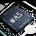
Apple A5 - Actually a Photoshop'd A4

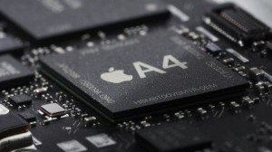
Today Apple announced the iPad 2, which unless you are living in a cave, you likely have heard about more then you wish already.  The iPad 2 debuts the next evolution in Apples own ARM processor.  The A4 (which was a single core 1GHz class ARM Cortex-A8 made by Samsung) is out, and a dual core replacement is in.  Details are thin until a proper tear down is done, but it is most likely a 1GHz dual core ARM Cortex-A9 with a dual core PowerVR 543 replacing the single core PowerVR 535.  It is most likely fab’d again by Samsung.  Apple’s press shot during their presentation is NOT an A5, the PR folks at Apple simply Photoshopped the original press shot of the A4 from last year. Note the date codes on the chip are 0939 and 0940 (sine their is 2 dies in it), which is late 2009.

Apple also made the somewhat deceptive remark that the iPad 2 is the first dual core tablet to ship ‘in volume.’  HP’s Touchpad runs a dual core Snapdragon and is shipping ‘soon.’  LG is shipping their tablet this month with a very capable Tegra 2, and Samsung will follow with the Galaxy Tab 10.1, also Tegra 2 powered.  RIM’s Playbook which is in beta, used a TI OMAP 4430 dual core Cortex-A9.  This puts Apple right in the mix of the dual core frenzy that will playout this year.

Apple A4 Press shot, notice the identical markings to the A5

We’ll update the photo as soon as someone (likely the folks at iFixIt) get and tear one down.

Tags:
, ,

Posted in:
Processor News