

|
|
|
| home | about | pictures | reference | trade | links |
How a CPU Microprocessor is made.
New Technologies
| Silicon on Insulator (SOI) | Silicon-on-Insulator (SOI)
SOI is by no means new. It was used on the RCA COSMAC 1802 in 1976.
This chip used Sapphire (Al2O3) for the insulator and ran at a then
blazing 6.4MHz. SOI or SOS technology has the added benefit of making
the chip less prone to radiation errors. This is why the RCA COSMAC
was used on the Pioneer, Voyager, and Galileo space probes. |
| Immersion Lithography | Immersion lithography is a projection enhancement
methodology that places a liquid between the lens and the wafer. The
additional refraction of the light passing through the liquid works
to enhance the resolution achievable by the projected light. IBM thinks
that the immersion litho process could enable 193 nm tools to produce
silicon circuit features as small as 45 nm, and maybe even smaller.
And to think there was a small industry gasp just over a year ago when
Intel announced it could stretch 193 nm tools to produce 65 nm transistor-based
chips. 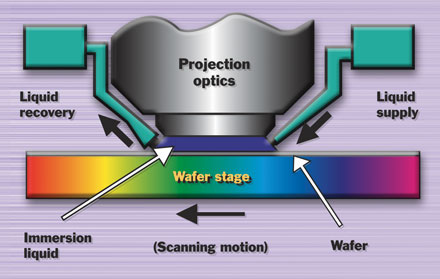 |
| Copper | Copper is a technology that is now generally in
wide use. Instead of using Aluminum interconnects and contact padsm
copper is now used. It has a lower resistance allowing for higher speeds
and lower power consumption.  |
| Low-K Dielectrics | Low-k dielectrics are used to form insulation between
interconnects in integrated circuits. The lower the k-value, the better
the insulator. The ideal insulator is air, which has a k-value of one.
However, it currently isn't feasible to make complex integrated circuits
with only air between the wires, a technique known as "silicon-on-nothing
(SON). As a result, researchers are examining dielectric materials that
are as porous as possible (to maximize the amount of air), yet durable
enough to withstand the rigors of the chipmaking process. Novellus has
introduced a material with a k-value of 1.7, which is considerably better
than the dielectric materials currently employed. Most dielectrics are
inserted onto chips by either spin-on processes or by Chemical Vapor
Deposition (CVD). Novellus uses a CVD approach for the dielectric material,
which the company claims is hard enough to withstand the chipmaking
process. The better the dielectric, the less space between wires. This
means smaller, faster parts. 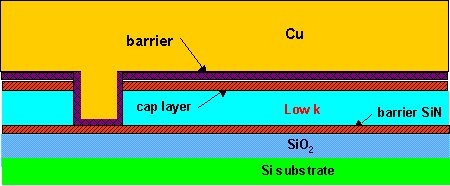 |
| Strained Germanium | Germanium has been used in smaller doses by several
companies, including IBM, in an existing manufacturing technique called
strained silicon. In this technique, a mixture of germanium and silicon
is placed next to a layer of pure silicon, which causes the silicon
atoms to stretch in order to align themselves with the silicon germanium
atoms. This opens a wider path that allows more electrons to flow through
the circuit. Researchers have long known that germanium is a better conductor of electricity than silicon, but they had not figured out how to build higher concentrations of germanium into chips using conventional techniques.. IBM has accomplished this, and has also figured out how to strain the germanium layer in order to further improve performance. Germanium, which is a by-product of zinc ore processing, is a hard element with the same crystal structure as a diamond. It is a semiconductor with electrical properties between those produced by a metal and an insulator. Its use as a transistor was key in the advancement of solid-state electronics. 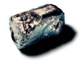 |
| EUV - Extreme UltraViolet | EUV is simply shorter wavelength (13nm) V process lithography. This allows for using masks to make smaller features. It is leading to X-ray lithography which is even shorter wavelength. |
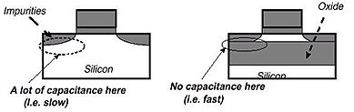
| Separation-by-IMplantation-of-OXygen (SIMOX) | Separation by Implantation of Oxygen (SIMOX) is a radically new fabrication
technique. SIMOX works by creating a perfectly smooth .15-micron layer
of silicon oxide SOI film. This new SOI film features virtually no imperfections
or impurities while retaining high yield rates. The SIMOX process involves
direct injection of purified oxygen into a silicon wafer at extremely
high temperatures. Under the high temperature, oxygen bonds with the silicon,
forming the thin layers of silicon oxide film. This relatively perfect
silicon oxide allows direct bonding to the pure crystalline silicon substrate. |
Continue to: Back to start
Making of Microprocessors 1 - 2
- 3 - 4