


|
|
|
| home | about | pictures | reference | trade | links |

AMD 29k (Streamlined Instruction Processor) ID Guide
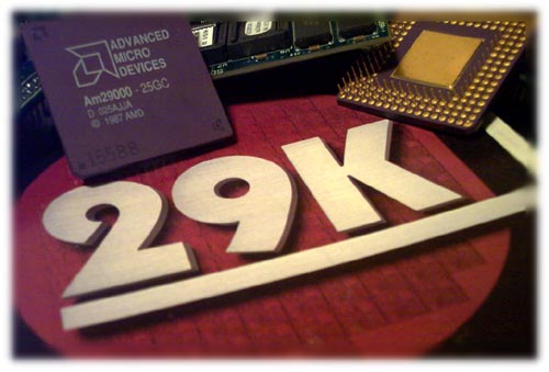
AMD 29K
The AMD 29000 is another load-store CPU descended from the
Berkeley RISC design (and the IBM 801 project), as a modern successor to the
earlier 2900 bitslice series (see
picture here) (beginning around 1981). Like the SPARC design that was
introduced shortly later, the 29000 has a large set of registers split into
local and global sets. But though it was introduced before the SPARC, it has
a more elegant method of register management.
The 29000 has 64 global registers, in comparison to the SPARC's eight. In
addition, the 29000 allows variable sized windows allocated from the 128 register
stack cache. The current window or stack frame is indicated by a stack pointer
(a modern version of the ISAR register in the Fairchild F8 CPU), a pointer
to the caller's frame is stored in the current frame, like in an ordinary
stack (directly supporting stack languages like C, a CISC-like philosophy).
Spills and fills occur only at the ends of the cache, and registers are saved/loaded
from the memory stack. This allows variable window sizes, from 1 to 128 registers.
This flexibility, plus the large set of global registers, makes register allocation
easier than in SPARC (optimised stack operations also make it ideal for stack-oriented
interpreted languages such as PostScript, making it popular as a laser printer
controller).
There is no special condition code register - any general register is used
instead, allowing several condition codes to be retained, though this sometimes
makes code more complex. An instruction prefetch buffer (using burst mode)
ensures a steady instruction stream. Branches to another stream can cause
a delay, so the first four new instructions are cached - next time a cached
branch (up to sixteen) is taken, the cache supplies instructions during the
initial memory access delay.
Registers aren't saved during interrupts, allowing the interrupt routine to determine whether the overhead is worthwhile. In addition, a form of register access control is provided. All registers can be protected, in blocks of 4, from access. These features make the 29000 useful for embedded applications, which is where most of these processors are used, allowing it at one point to claim the title of 'the most popular RISC processor'. The 29000 also includes an MMU and support for the 29027 FPU. The superscalar 29050 version in 1990 integrated a redesigned FPU (4 instructions could be dispatched to execute out of order and speculatively).
In late 1995 Advanced Micro Devices dropped development of the 29K in favour of its more profitable clones of Intel 80x86 processors, while Intel tried to replace the x86 with an architecture similar to the 29K, although much of the development of the superscalar core for a new AMD 29000 (including FPU designs from the 29050) was shared with the 'K5' (1995) Pentium compatible processor (the 'K5' translates 80x86 instructions to RISC-like instructions, and dispatches up to five at once to two integer units, one FPU, a branch and a load/store unit).
The AMD 29K series of 32 bit microprocessors were designed to directly compete
with the Intel 80960 and Motorola MC68020/030. They are faster at most operations
(clock for clock) then the competition and were extensively used. There were
many variations of the architecture (including a 16bit MCU and FPU). This,
like the 80960, makes collecting difficult. Below
is a comprehensive guide to the differences in these CPUs. The 29050 is the
direct predecessor or the K5
x86 CPU. The K5 translates x86 into RISC 29k instructions.

3-Bus Microprocessors
2-Bus Microprocessors
Microcontrollers
Additional 29K Devices and Support
Honeywell and the 29050
3-Bus Microprocessors
29K 3-bus microprocessors included the 29000, 29005 and 29050. They have seperate
buses for data, addresses and instructions. All three of these CPUs are pin
compatible and are 5 Volt devices. The 29005 was the value chip with the 29050
being the premier microporcessor. Thee 29050 possed a very capable FPU. It
was a VERY capable processor and is still in wide use today.
| Features | Am29005 |
Am29000 |
Am29050 |
| Buses (32 bit) | Address Instruction Data |
Address Instruction Data |
Address Instruction Data |
| Data Cache | No |
No |
No |
| Instruction Cache | No |
BTC 32 x 4 Words (512 bytes) |
BTC 128 x 2 or 64 x 4 (1 Kbyte) |
| Cache Associativity | - |
2 Way |
2-Way |
| Integer Multiplier | Software |
Software |
32 x 32 bit |
| JTAG Debug Support | No |
No |
No |
| HW Breakpoints | No |
No |
Instruction |
| Scalable Clocking Technology | No |
No |
No |
| Programmable Bus Sizing | No |
No |
No |
| OnChip ROM access Support | x32 |
x32 |
x32 |
| Regsiter Set: Total Data Registers* Local Registers Global Registers |
192 128 64 |
192 128 64 |
196 128 68 |
| On-Chip FPU | No |
No |
Yes |
| On-Chip MMU | No |
Yes |
Yes |
| On-Chip Large Region Mgmt. | No |
No |
Yes |
| Max Data/Instruction Burst (bytes) | 1K/1K |
1K/1K |
1K/1K |
| On Chip Interrupt Controller | Yes |
Yes |
Yes |
| Interrupt/Trap pins | 6 |
6 |
6 |
| On-Chip Timer | Yes |
Yes |
Yes |
| Endian | Both |
Both |
Both |
| Operating Voltage: Vcc I/O Tolerance |
5V 5V |
5V 5V |
5V 5V |
| Clock Speeds |
16 |
16,20,25,33,40 |
20,25,33,40,50 |
| Packages: CPGA (GC Suffix) PQFP (KC Suffix) CerQuad |
N/A 168 N/A |
169 168 (16 / 20MHz) N/A |
169 N/A N/A |
| Pictures | Am29000-16GC Am29000-25GC-ES |
AM29050-40GC |
| Features | Am29035 |
Am29030 |
Am29040 |
| Buses (32 bit) | Address Combined Instruction / Data |
Address Combined Instruction / Data |
Address Combined Instruction / Data |
| Data Cache | No |
No |
4K |
| Instruction Cache | 4K |
4K |
4K |
| Cache Associativity | Direct Mapped |
2 Way |
2-Way |
| Integer Multiplier | Software |
Software |
32 x 32 bit |
| JTAG Debug Support | Yes |
Yes |
Yes |
| HW Breakpoints | No |
No |
Instruction and Data |
| Scalable Clocking Technology | Yes |
Yes |
Yes |
| Programmable Bus Sizing | Yes, 16/32bit |
Yes, 16/32bit |
Yes, 16/32bit |
| OnChip ROM access Support | x8, x16, x32 |
x8, x16, x32 |
x8, x16, x32 |
| Regsiter Set: Total Data Registers* Local Registers Global Registers |
192 128 64 |
192 128 64 |
192 128 64 |
| On-Chip FPU | No |
No |
No |
| On-Chip MMU | Yes |
Yes |
Yes |
| On-Chip Large Region Mgmt. | No |
No |
Yes |
| Max Data/Instruction Burst (bytes) | 1K/1K |
1K/1K |
1K/1K |
| On Chip Interrupt Controller | Yes |
Yes |
Yes |
| Interrupt/Trap pins | 6 |
6 |
6 |
| On-Chip Timer | Yes |
Yes |
Yes |
| Endian | Both |
Both |
Both |
| Operating Voltage: Vcc I/O Tolerance |
5V 5V |
5V 5V |
3.3 V 5V |
| Clock Speeds | 16 |
20,25,33 |
33,40,50 |
| Packages: CPGA PQFP CerQuad |
N/A N/A 144 |
145 N/A 144 (20 & 25 MHz) |
145 144 (33 MHz) N/A |
| Pictures | Am29030-25FC Am29030-25GC |
Am29040-50GC-ES Am29040-33GC |
| Features | Am29205 |
Am29202 |
Am29200 |
Am29245 |
Am29240 |
Am29243 |
| Instruction Cache | - |
- |
- |
4K |
4K |
4K |
| Data Cache | - |
- |
- |
- |
2K |
2K |
| Cache Associativity | - |
- |
- |
2-Way |
2-Way |
2-Way |
| Integer Multiplier | Software |
Software |
Software |
Software |
32 x 32 bit |
32 x 32 bit |
| MMU | - |
- |
- |
1 TLB 16 Entry |
1 TLB 16 Entry |
2 TLB 32Entry |
| Data Bus Width Internal External |
32 16 |
32 32 |
32 32 |
32 32 |
32 32 |
32 32 |
| ROM Banks Width ROM Size (Max/Bank) Boot-Up ROM Width Burst-Mode Access |
3 8, 16 4M 16bits No |
4 8, 16, 32 4M 8, 16, 32 No |
4 8, 16, 32 16 M 8, 16, 32 Yes |
4 8, 16, 32 16 M 8, 16, 32 Yes |
4 8, 16, 32 16 M 8, 16, 32 Yes |
4 8, 16, 32 16 M 8, 16, 32 Yes |
| DRAM Interface Banks Width Size: 32bit Mode Size: 16-bit Mode Video DRAM Initial/Burst Access Cycles |
4 16 - 8M No 3/2 |
4 16, 32 16M 8M No 3/2 |
4 16, 32 16M 8M Yes 3/2 |
4 16, 32 16M 8M Yes 2/1 |
4 16, 32 16M 8M Yes 2/1 |
4 16, 32 16M 8M No 3/2 |
| DRAM Parity | No |
No |
No |
No |
No |
Yes |
| DMA | 8, 16 bits |
8, 16, 32 bits |
8, 16, 32 bits |
8, 16, 32 bits |
8, 16, 32 bits |
8, 16, 32 bits |
| Double Frequency Option | No |
No |
No |
No |
Yes |
Yes |
| Low Voltage Operation | No |
No |
No |
Yes |
Yes |
Yes |
| PIA Ports Data Width Min Access Cycles |
2 8, 16 3 |
2 8, 16, 32 3 |
6 8, 16, 32 3 |
6 8, 16, 32 1 |
6 8, 16, 32 1 |
6 8, 16, 32 1 |
| PIO Signals Signals for Interrupt Gener. |
8 8 |
12 8 |
16 8 |
16 8 |
16 8 |
16 8 |
| Serial Ports | 1 |
1 |
1 |
1 |
2 |
2 |
| Interrupt Pins | 2 |
2 |
4 |
4 |
4 |
4 |
| Parallel Port Controller 32-bit Transfer IEEE1284 |
Yes No No |
Yes Yes Yes |
Yes Yes No |
Yes Yes No |
Yes Yes No |
Yes Yes No |
| JTAG Debug | No |
Yes |
Yes |
Yes |
Yes |
Yes |
| Serializer/Deserializer | Yes |
Yes |
Yes |
Yes |
Yes |
No |
| Package | 100PQFP |
132PQFP |
168PQFP |
196PQFP |
96PQFP |
96PQFP |
| Operating Voltage Vcc I/O Tolerance |
5V 5V |
5V 5V |
5V 5V |
3.3V or 5V 5V |
3.3V or 5V 5V |
3.3V or 5V 5V |
| Clock Speeds | 12, 16MHz |
12, 16, 20 |
16, 20 |
16 |
29, 25, 33 |
29, 25, 33 |
Additional 29K Devices and Support
AMD made an external FPU (actually an arithmetic accelerator) for the 29K
but it was quickly superceded by the onboard FPU of the 29050. The 2911x series
of microcontrollers is unrelated to the normal 29k family but is interesting
none the less, if anything for the remarkable package it came in.
| Device | Speed | Voltage | Type | Data Bus Width |
Inst. Cache |
Data Cache |
Packages | Notes |
| 29027 | 16, 20, 25 | 5V | FPU | 32 | 0KB | 0KB | FPU for 29K | |
| 29116 | 10 | 5V/3.3V | MCU | 16 | 0KB | 0KB | 52 DIP 68 PLCC |
29116DC 29C116- 2JC |
| 29117 | MCU | 16 | 0KB | 0KB | 52 DIP | |||
| 29325 | FPU | 32 | 0KB | 0KB | ||||
| 29332 | ALU | 32 | 0KB | 0KB | ||||
| 29327 | FPU | 32 | ||||||
| 29501A | Multi-Port Pipelined Processor (Byte-Slice™) | BSP | ||||||
|
Device |
29K Support Devices |
| Am29041 | Data transfer controller |
| Am29062 | Integrated cache unit with 8K bytes RAM |
| Am29323 | 32-Bit Parallel Multiplier |
| Am29331 | 16-Bit Microprogram Sequencer |
| Am29334 | Four-Port, Dual-Access Register File |
| Am29360 | 32-Bit Error Detection and Correction Unit |
| Am29368 | 1M-Bit Dynamic Memory Controller (DMC) |
AMD discontinued the 29K series completely in 1995. This is most likely due to the development of the K5 and K6 processors. There were some issues with discontinuing the 29K as many were being used in mission critical fields (aviation mainly). To avoid hasseling with the FAA and having to provide support for a product they no longer were going to make, AMD sold the 29050 design to Honeywell, a well known aerospace and defense company.
Honeywell used and still uses the 29050 (implemented in an ASIC) in its Versatile Integrated Avionics package (known as a VIA). The VIA is responible for data logging, data display, and control of many subsystems on an aircraft. Each section (Core Proccessing Module - CPM) of a VIA implements a pair of 29050s (HI-29KII as they are known at Honeywell). The CPUs are setup in a system known as voting. All outputs (address, data and control) are ran through a comparator, if each CPU sends out the same signals then the system continues. if the signals do NOT match then there is a fault, and the sytem enters an error mode where it logs the error, and attempts to recover. This is a very common set-up on a mission critical device such as flight computers.
Currently the following planes implement a VIA using the 29050:
|
Yes the tiny AMD 29050 Keeps THIS in the air:

Back to Top
If you know of any more 29k info etc. Please e-mail me and I will add it.
Thanks to R. Brians of Epsilon Industries for providing much of my 29K material.