August 8th, 2016 ~ by admin

Intel MCS-86 Test Systems now available.

MCS-86 Test Boards For SaleThe CPU Shack is pleased to now offer test systems for testing the famous Intel 8086 and 8088 processors.  They also support testing of the 8087 FPU, as well as the NEC variants (V20/V30).  As an added bonus, an expansion is included for testing the i186/i188 processors as well.

Of course the original NMOS,  and later CMOS versions are supported from many manufacturers.

Head on over to the MCS-86 Test System page for more information and to order your system.


Posted in:
Products

July 11th, 2016 ~ by admin

Sparkplugs, O-Scopes and Cell Phones…

AMD 486 processor. Note the logo in the lower right corner. Package is from Kyocera (Click for larger version)

AMD 486 processor. Note the logo in the lower right corner. Package is from Kyocera (Click for larger version)

What do all 3 of these things have in common? And what in the world do they have to do with computer processors (ok modern oscilloscopes and cell phones DO have CPUs in them but spark plugs?). Tektronix was started here in Oregon in 1946 making oscilloscopes and other test equipment.  Throughout the last 70 years they have continued to do so, but along the way they also began to make everything needed to manufacture the final equipment they sold.  Design/simulation software, PCB manufacturing, IC manufacturing, displays, and even the packaging used for IC’s.  In recent years many of these vertically integrated operations have been spun off, but they do still maintain some.

Tektronix packaging options from the early 1990's (Click for larger version)

Tektronix packaging options from the early 1990’s (Click for larger version)


When an IC manufacturer (such as Intel, AMD, etc) designs/builds an IC what they typically are creating (or having made in the case of fabless companies) is the silicon die itself.  This little piece of silicon contains the millions of transistors needed to perform whatever task its made for, but for most uses that silicon die needs to be packaged to be useful.  A sliver of silicon is hard to work with and integrate into designs, a package provides the routing of wire/leads to the die, as well as protects it from the environment, while dissipating any heat it generates.

IC manufactures do not typically make their own packages, they are either contracted out or bought off the shelf.  Tektronix is one of several companies that makes and sells IC packages.  The pictured display is a sample of some of the packaging types they offered.  You can recognize some of the more common packages, as well as some more specialty ones such as the ‘POWER TAB’ that was used in analog equipment frequently (like audio amplifiers etc).

Anam/Amkor Test package

Anam/Amkor Test package

Tektronix isn’t the only company that offers packages for IC.  Perhaps the two largest are NGK and Kyocera.  Both have extensive experience with ceramics, a material very useful in IC packages.  Developing high strength, high temperature ceramics for spark plugs, isn’t so much different from designing the same for a high end processor.  Kyocera started life making ceramic insulators, well before ever getting into cell phones (in 2000) and ceramic packaging continues to be their core business.

Often times assembly and test of a IC is handled by yet another company.  Many companies (such as Amkor) entire business is based on taking IC dies from one company, assembling them into packages from another, testing them, and shipping them.  So next time you look at a CPU and read its makers name boldly written on its top, there is a good chance that that name had but one part in that IC.

July 3rd, 2016 ~ by admin

Juno Joins Jupiter: And Brings Some Computers For The Trip

Juno - RAD750 Powered Mission to Jupiter

Juno – RAD750 Powered Mission to Jupiter

NASA’s Juno mission to Jupiter arrives in just about a day, after a 5 year journey that began in August of 2011 aboard an Atlas V rocket.  The Juno mission is primarily concerned with studying the magnetic fields, particles, and structure of Jupiter.  Finding out how Jupiter works, and what its core is made of are some of Juno’s goals.  None of the experiments need a camera, but NASA decided, in the interest of public outreach and education, that if you are going to spend $1 billion to send a probe to Jupiter, it probably should have a camera.  Energetic particle detectors, Magnetometers, and Auroral Mappers are great for science, but what the public is inspired by is pretty pictures of wild and distant worlds.

Juno is powered by a now familiar computer, the BAE RAD750 PowerPC radiation hardened computer.  It operates at up to 200MHz (about the processing power of a mid 1990’s Apple Computer) and includes 256MB of Flash memory and 128MB of DRAM.  It (and the other electronics) are encased in a 1cm thick titanium radiation vault.  Flying in a polar orbit around Jupiter, Juno will experience intense radiation and magnetic fields.  The probe is expected to encounter radiation levels in the order of 10Mrads+.  The vault limits this to 25krads, within what the electronics can handle.  It should be noted that a dose of 10krads is fatal in most cases.  This intense of radiation will degrade the prober, even with shielding, resulting in a mission life of only 37 orbits (a little over a year) before the probe will be gracefully crashed into Jupiter.

Read More »

July 1st, 2016 ~ by admin

Signetics 2650 Test Boards Now Available

Signetics 2650 Test Board For SaleContinuing our goal of having test boards available for pretty much every common architecture of the 1970’s we now have a board available for testing Signetics (and later Philips) 8-bit NMOS processor, the 2650, 2650A and 2650B.  Made on a cool black PCB they are a fairly simple system, but are capable of testing some of the special features of the 2650 as well as the added features of the 2650B (if anyone happens to locate one)

These chips did not achieve the wide microcomputer success hoped for (likely due to a lack of second sourcing) they did find their way into many industrial/embedding systems, as well as many arcade/video games (including some made by ATARI).

These boards are in stock, and ship world wide for $94.95.  Head on over to the 2650 page to grab one.

Posted in:
Products

June 21st, 2016 ~ by admin

Fujitsu to take ARM into the realm of Super

Fujitsu MB86900 - Original SPARC Processor from 1987

Fujitsu MB86900 – Original SPARC Processor from 1987 – 14.28MHz

Back in 1987 Fujitsu was one of the founders of the SPARC RISC architecture.  The very first SPARC processors were built by Fujitsu, and used in their servers through the 1990’s and 2000’s. SPARC processors were first used in the CM-5 Thinking Machine in 1991 using 1024 SPARC processors (later upgraded to SuperSPARCs).  Fujitsu began making supercomputers based on SPARC in 1992 with the AP1000 and its UltraSPARC based successor the AP3000.  One of their latest, the K machine, is a 705,024 core 12MW SPARC64 VIIIfx based design that ranks as #5 on the Top 500 Supercomputer list.

This is why its a surprise to many that they have announced the successor to the K Machine will be similar in topology, and will be RISC based, but will not be SPARC based, rather Fujitsu has been working with another well known RISC architecture with serious HPC aspirations, ARM.  Fujitsu has been an ARM architecture license holder for some time and the post-K machine will be based on the 64-bit ARMv8 architecture.  ARM has been working hard to make their chips appeal to the datacenter environment, with some success.  Their low power consumption makes them ideal for high density applications, which a super computer needs.  Estimated performance is 1,000 Peta FLOPS and it is due to go into service in 2020. A speed that would eclipse another recently announced RISC supercomputer….

Read More »

Posted in:
Processor News

May 21st, 2016 ~ by admin

Azul Systems Vega 3: 54 Cups of Coffee

Azul Systems V03A0L1-Vega 3 - 54-core RISC Java Processor

Azul Systems V03A0L1-Vega 3 – 54-core RISC Java Processor

Azul Systems was started in 2002 to do what anyone who has used Java wishes it to be, make it faster, and more scalable.  Azul did this using both software (optimized Java compilers/Run time environments) and hardware.  The Vega processor line was Azul’s attempt at a hardware acceleration of Java.  This wasn’t a new concept, many companies have created hardware implementations to execute Java.  Notable is the Jazelle extentions from ARM, which can directly execute Java byte-codes and Sun developed the pico.Java processor to do similar.  The Vega takes a rather different route though.  Azul found that direct execution of Java byte codes wasn’t really that important if you had very efficient JIT (Just In Time) compilation to an efficient architecture.  This allows the processor to be a bit more adaptable as you now have a layer between the hard to change hardware, and the Java feeding it.  New instructions, or work arounds/speed up become easier to implement.

The Vega 3, the last of the Vega series is a 54-core processor, each core is a classic 3-address 64-bit RISC processor with 32 registers and 16K of Instruction cache + 16K of Data cache.  The architecture is designed to be ‘Java friendly’  with fairly weak memory model for easier scaling, support for more robust garbage collection, and not a large focus on FPU performance. There is 12MB of L2 cache on chip as well (each 9-cores share 2M). The chips are fab’d by TSMC on a 65nm or 90nm process (it isn’t clear which from Azul’s documentation).  All registers and caches support ECC, and the chips themselves self-report any problems, allowing the system (which may use up to 16 chips (864 cores) to disable any misbehaving processor or memory).

Vega 3 - 54-core die.  Truly massive die.  Software though allows workaround for many hardware defects.

Vega 3 – 54-core die. Truly massive die. Software though allows workaround for many hardware defects.

The Vega 3, and the systems it was used in, allowed Java to be scaled to much larger heap sizes (500G+) and core counts, without coherency problems.  Many institutions (especially financial) still use Java programs that were written long ago, recoding them would speed them up, but that is not practical.  The Vega3 (and other Azul products) allow old code, to be ran faster with no modifications.

Azul sold many systems running the Vega processors but eventually moved to software only solutions, that could efficiently run Java on existing x86 hardware.  The methods though are similar, just no longer the need for custom hardware to run it on.  Azul appliances can be added to any datacenter to catch and accelerate Java applications.

Azul wasn’t the first company to accelerate Java, and they certainly won’t be the last.  Java’s simplicity and platform independence will keep it around, and the ability to run decades old code fast and safely on modern hardware will continue to drive products.  Its like COBOL all over again…

Tags:
,

Posted in:
CPU of the Day

May 16th, 2016 ~ by admin

National Semiconductor SC/MP Test Boards Now Available

National Semi SC/MP Test Board

National Semi SC/MP Test Board

National Semiconductor released the SC/MP (aka the SCAMP or ISP-8A-500) in 1974 as a low cost PMOS 8-bit processor.  Later the design was moved to an NMOS process resulting in higher clock speeds and simpler power supply requirements.  This version was known as the SC/MP II or the ISP-8A-600.  It was used well into the 1980’s.

This test board is designed to test with the PMOS or the NMOS versions of this chip.  It has power supplies and clocking for both the PMOS and NMOS versions and requires only the slide of a switch to change between them.

I have a couple in stock, $94.95 with FREE shipping.

More info and purchasing info on the SC/MP Test Board page.

April 28th, 2016 ~ by admin

The Evolution of the Intel 8051 Processes

Intel C8051-3 - 1981 - Original 3.5u HMOS-E

Intel C8051-3 – 1981 – Original 3.5u HMOS

That’s not a typo, we’re going to look briefly at the technology processes (rather then the processors themselves)  Intel went through in the first 5 years of the MCS-51 microcontrollers, and the exceedingly confusing nature of the resulting naming.  When the Intel 8051 series was released in 1980 it was made on two different processes.  The 8031/8051 (non-EPROM) were made on the HMOS-I process, a 3.5 micron single poly process.

Intel C8751-8 - 1982 - Orignal 3.5u HMOS-E

Intel C8751-8 – 1982 – Orignal 3.5u HMOS-E

The EPROM version, the 8751 was made on an EPROM process, HMOS-E, which was still a 3.5 micron process, but with 2 poly layers.  This resulted in some slight differences in electrical characteristics (not to mention the programming features not needed on the MaskROM and ROMless versions.

Intel 8751H B-2 ENG. SAMPLE - 1985 -HMOSII-E - 2u

Intel 8751H B-2 ENG. SAMPLE – 1985 -HMOSII-E – 2u

Intel then moved to the HMOS-II (Intel Process P414.1) process in 1984.  This was a shrink to 2 microns, and the EPROM version was also shrunk, but again, using a slightly different EPROM process (Intel Process P421.X).  The HMOSII MaskROM and ROMless versions received the suffix AH, ‘A’ denoting a minor update to the architecture, and ‘H’ for the new HMOSII process.  The EPROM version did not see the same updates though, it received EPROM security bit support and was simply called the 8751H.

Read More »

Tags:

Posted in:
CPU of the Day

April 14th, 2016 ~ by admin

DEC NVAX++ NV5: The End of VAX

DEC NVAX 21-34457-05 246B - 1992  -71MHz

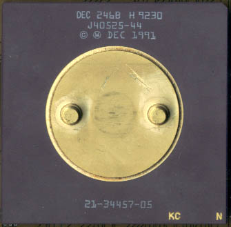
DEC NVAX 21-34457-05 246B – 1992 -71MHz

About a year ago we covered the DEC RIGEL VAX Processor.  After The RIGEL DEC moved to make a single chip VAX processor that would include the CPU, FPU, and cache controller on one single die.  Work on the design began in 1987, and first silicon shipping in 1991.  Performance ended up being as good or better then the very high end VAX 9000 systems (implemented in ECL logic).

The original NVAX processor was made on a 0.75u 3-Layer CMOS process (DEC CMOS-4) and contained 1.3 million transistors in a 339 pin CPGA package.  Initial clock speed, in 1991 was 71MHz.  NVAX was then the fastest CISC processor made.  Speeds ramped up to 90.9MHz at the high end and a lower end of 62.5MHz. The first NVAX models were identified as 246B and 246C. Later versions, made well into 1996, were made on the CMOS-4S process, a 10% shrink to 0.675u and were labeled 1001C.

Internally NVAX was very familiar, the FPU was largely reused directly from RIGEL.  The NVAX also maintains the 4-phase clocking scheme from RIGEL, but moves the clock generator on chip. It also maintained the 2K of on die instruction cache from RIGEL, but added a 8K data/instruction mixed cache as well.  An L2 cache was supported in sizes of 256K 512K 1M or 2M, and located off chip.  The NVAX continued the 6-stage pipeline of RIGEL with some enhancements.  One of the greatest performance enhancements over RIGEL is the handling of pipeline stalls.  In the RIGEL pipeline, a stall in one stage would stall the entire pipe line, whereas on NVAX, in most cases, a stall in one stage does not prevent the other stages from continuing.

At nearly the same time as the development of the NVAX DEC was also developing a competitor to MIPS, a RISC architecture.  This new RISC architecture was codenamed EVAX, for Enhanced VAX, and was a purely RISC architecture that could run translated VAX CISC code with very little performance penalty.  It did however borrow from VAX, like the NVAX, EVAX used the FPU from the RIGEL. DEC went on to brand the EVAX as Alpha AXP, to separate it from the VAX line, though its internal naming of EV4, EV5 etc was left intact, as the last remnant of VAX.

DEC 2140568-02 299D NVAX++ 170.9MHz - 1996 - from a VAX7800

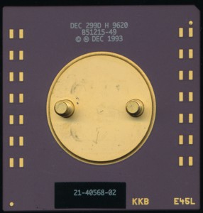
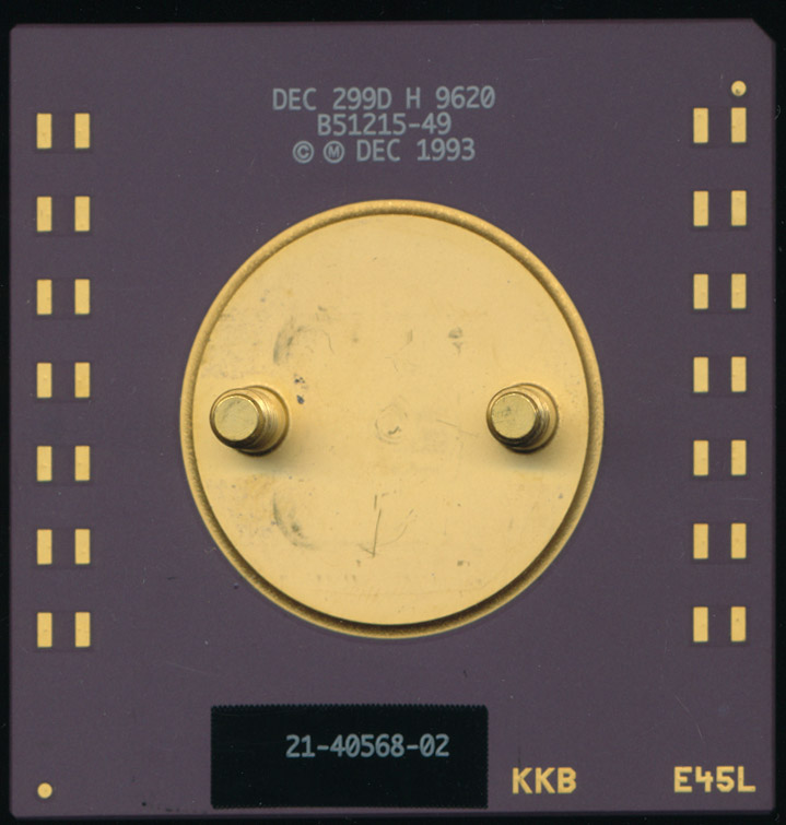
DEC 21-40568-02 299D NVAX++ 170.9MHz – 1996 – from a VAX7800

Having two high performance processor types at the same time left DEC in a bit of a dilemma so they created a third, known as the NVAX+ (DEC 262D).  The NVAX+ was originally made on the same CMOS-4 process as the NVAX and ran at 90.9MHz.  The NVAX+ was meant to be a bridge between the VAX line and the Alpha AXP.  It was a NVAX core, wrapped in an EVAX (Alpha AXP) external interface, it was made in the same 431PGA as the Alpha 21064 and was pin for pin compatible, the same board could be used for either.  It supported more L2 cache then the NVAX, supporting six cache sizes (4MB, 2MB, 1MB, 512KB, 256KB, 128KB),

In 1994 the NVAX+ was shrunk to the DEC CMOS-5 4-Layer 0.5 micron process resulting in the NVAX++ (DEC 299D) which ran from 133-170.9MHz.  These speeds continued to be the fastest CISC processors until Intel released the Pentium Pro at 180 and 200MHz in 1996.  Ultimately Intel’s dominance, and the coming dominance of RISC performance were the writing on the wall, and the VAX, and not long after it DEC itself were doomed to reside in the history books.  By 1997 The NVAX++ was off the market.  In 1997 the DEC Alpha team was operating out of offices owned by Intel (who also took over DEC’s fab’s), and in 1998 the remains of DEC, and the Alpha team, were bought by Compaq. And by 2004 Alpha was phased out in favor of Itanium (a now rather ironic decision by HP/Compaq).
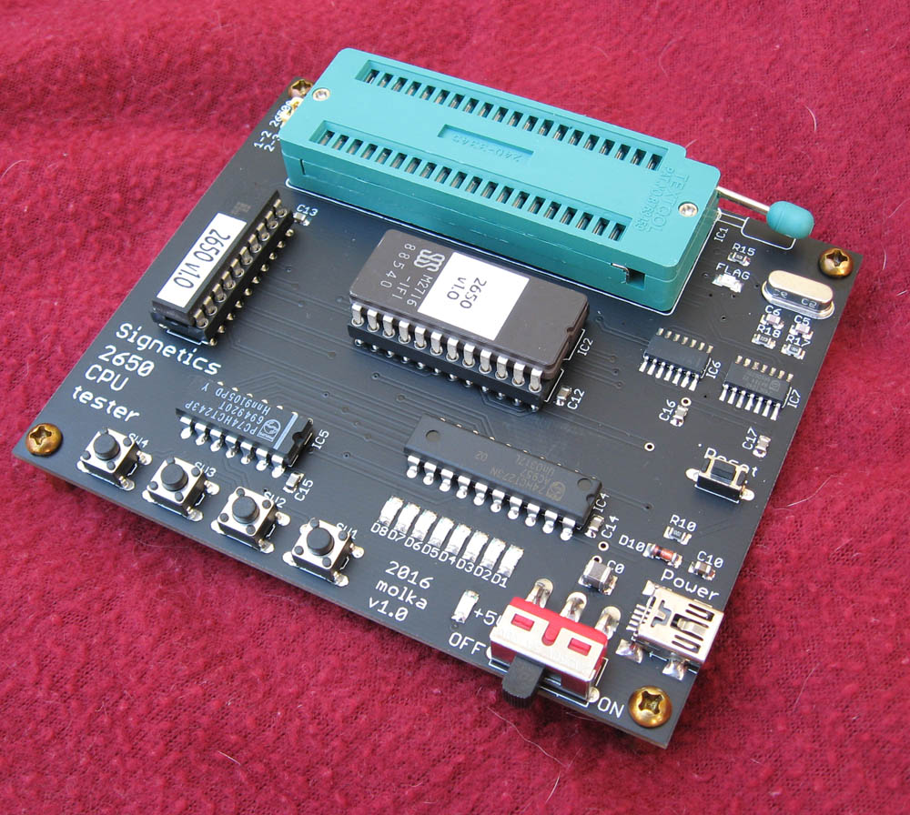
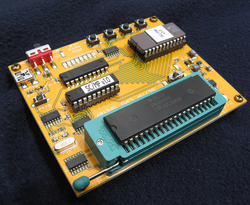
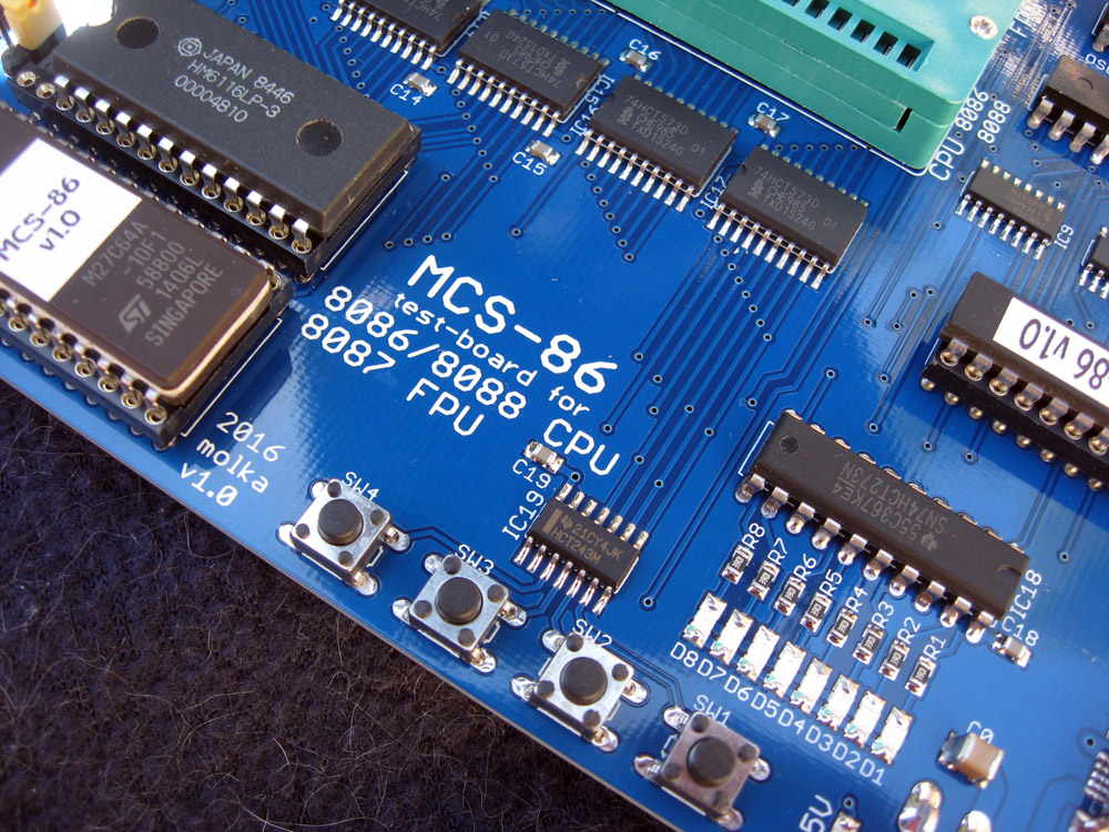
 

Tags:
, , ,

Posted in:
CPU of the Day

March 24th, 2016 ~ by admin

Intel MCS-4/40 Test Boards Back in Stock and More Testers to Come

I finally got more of the Intel MCS-4/40 Test Boards ready to ship.  Grab yours soon if you want one.  All other test boards are in stock too, including the RCA COSMAC boards, the Intel MCS-8 board and the Intel MCS-80 board (with Z80 8085 and NSC800 Expansions.

New Test Boards:  Coming soon will be two new test board types.  First is a board for the SC/MP and SC/MP II CPUs made by National Semiconductor. The second is a whole test system, designed to test Motorola 680x processors as well as MOS 650x processors and many of their derivatives.  All told it’ll test over 30 different chip types!  Even some of the more unusual/special versions.  Commodore 6510? Yup! Nintendo Ricoh? Yup! and a whole lot more…

Coming Soon!

Posted in:
Products