
IBM z800 MCM Mainframe Processor
IBM z800 MCM
Mainframes are the workhorses of the computing industry. They process transactions for about every industry, and handle the brunt of the economy. Their MTBF (Mean Time Between Failures) is measured in decades (typically 20-50 years). A comparison to a home computer is hard to make, they are in an entirely different league, playing an entirely different game.
Data Intense vs. CPU Intense
Mainframe processors such as these work in what is referred to as ‘Data Intensive’ computing environments. This is different from multi-cored processing that focuses on ‘CPU Intensive’ computing. CPU intense has a relatively small data set, but most perform a lot of work on that set of data, or do the same instruction on a set of data (such as graphics). CPU Intense processing can often be sped up with the addition of more processing cores. Data Intense processing does not see as much benefit from adding cores. Its biggest bottleneck is accessing the data, thus the System z tends to have VERY large caches, and very high bandwidth memory. They typically operate on transactional type data, where the processing has to operate in a certain order (A has to be done before B which has to finish before C etc).
IBM was one of the first, and continues to be one of the largest suppliers of such systems. Starting with the System/360 introduced in 1964 to the zSeries today. The zSeries was first launched in 2000 with the z900, a significant upgrade from the System/390. Data addressing was moved to 64-bits (from 31 bits) yet backwards compatibility (all the way back to the 360) is maintained. The z900 ran at 775MHz and was built with a 35 die MCM containing 20 Processing Units (PUs) and 32MB of L2 Cache.
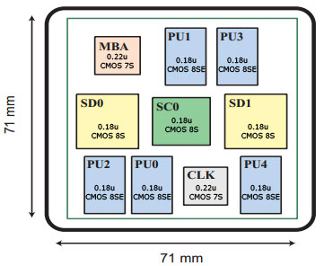
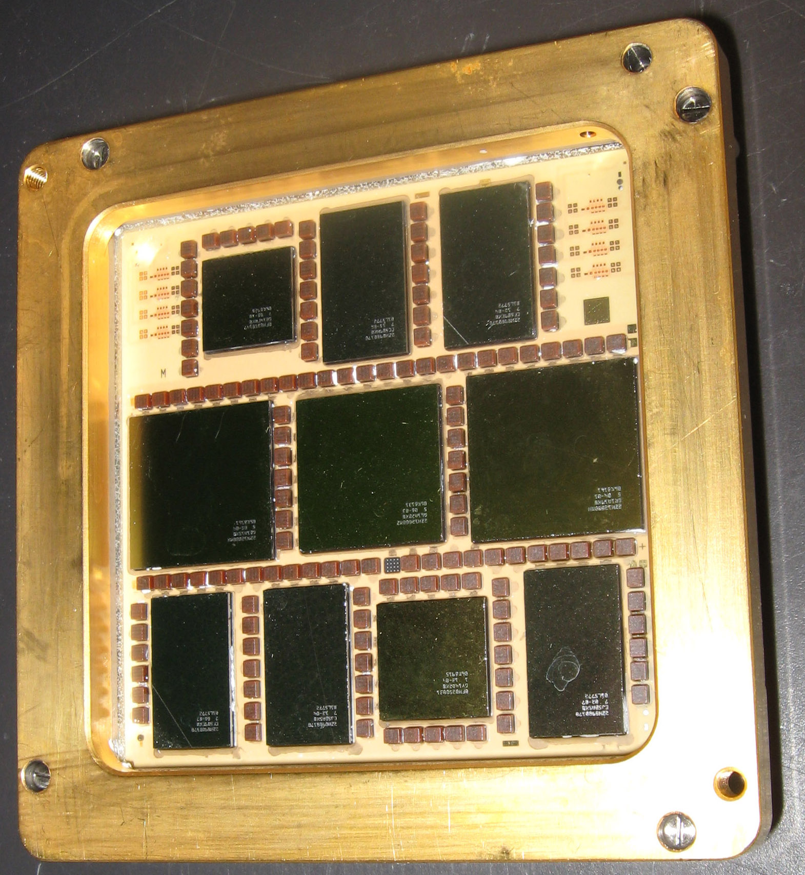
z800 MCM Layout (click to enlarge)
The IBM z800
In 2002 IBM released the z800 which was to be for small to medium businesses. This meant that it would have a somewhat lower performance, but also needed to be much less expensive. The z800 is manufactured with a 10 chip MCM. This contains 5 PUs (one of which is dedicated as a System Administration Processor) and 8MB of L2 Cache. Each of the 5 PUs contains 512KB of L1 Cache (split between Data and Instruction). Clock speed is 625MHz. Each PU chip contains 44 Million transistors and is manufactured on IBMs copper 0.18u CMOS 8SE process. The 2 4MB cache chips each contain 234 Million transistors and are also made on a 0.18u process (in this case CMOS 8S, slightly less dense then 8SE). The MCM also contains a Storage control chip (0.18u) a CLK driver (0.22u CMOS 7S) and a MBA (Memory Bus Adapter, also 0.22u). These are all packages on a single 42 layer glass-ceramic thin film MCM.
Each PU chip physically contains 2 separate cores. This is not to increase performance, but to increase reliability. Both cores execute the same instructions, and compare the results. If the results differ, the PU automatically retries the the instruction. If it again fails, the PU is shut down, the load is shifted to the other PUs (or the spare PU is activated if not already) and an IBM service technician is automatically notified. This is all seamless, and software independent. On larger systems (like the z900) nearly every component, including the processor can be changed out, while the mainframe is running, with no effect on processing. Memory, processor books, power supplies, I/O, cooling, is all hot-swappable. Restarting a mainframe is simply not acceptable or allowable.
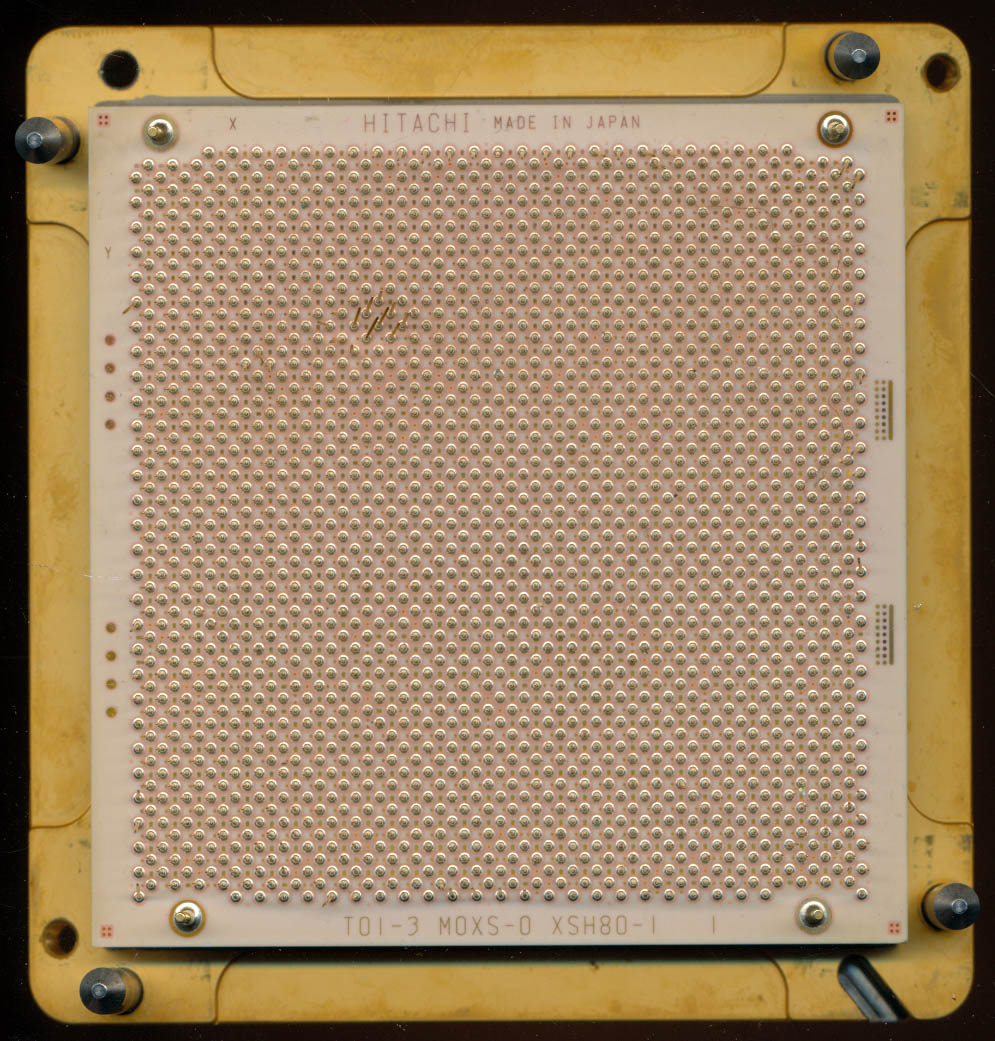
z800- Made in Japan by Hitachi
Made in Japan
The pin side of the z800 MCM is labeled ‘Hitachi – Made in Japan.’ In fact, no where on the IBM z800 MCM is it marked ‘IBM.’ Certainly ironic considering that for some time IBM and Hitachi were competitors in the mainframe market. Why then would an IBM system be labeled Hitachi? In 2000 Hitachi decided to shift their focus to storage systems rather than mainframes. About the same time they began an extensive cooperation with IBM on MCM design. The result? The z800 and later version of the z900 MCMs. Hitachi was able to manufacture ceramic MCMs with a finer via pitch, meaning the connections between the several dozen layers of the substrate could be much closer together, resulting in less layer, and less wiring, in the end, cheaper and more reliable. Considering a z900 MCM has nearly a kilometer of wiring in it, any reduction was a good thing. Marking the MCMs Made in Japan (most of the MCM IS made In Japan) was hoped to help bring Hitachi’s former mainframe customers to IBM systems.
IBM continues to innovate in mainframes, bringing more and more data processing power to the System z mainframes. Clock speeds well over 4GHz are standard on the z196s. This all while maintaining extreme reliability.
March 12th, 2014 at 4:07 pm
“8MB of L3 Cache”
Did you mean L2 cache (corresponding to the “32MB of L2 Cache” in the z900)? (With 0.5 MiB of L1 caches per PU and 5 PUs, 8 MiB also looks more reasonable for a shared L2.)
March 12th, 2014 at 4:14 pm
yah no L3 on it, fixed.
December 3rd, 2017 at 1:40 pm
how much would you sell that or IBM z900 CPU
December 3rd, 2017 at 2:23 pm
I don’t have a spare to sell I don’t think
December 3rd, 2017 at 4:42 pm
would you send me photos of the one you have.I would appreciate.
December 4th, 2017 at 2:19 am
Sent you some
Here is one on eBay too
https://rover.ebay.com/rover/1/711-53200-19255-0/1?ff3=4&toolid=11800&pub=5575061345&campid=5337623773&mpre=https%3A%2F%2Fwww.ebay.com%2Fitm%2Fvintage-rare-collectible-IBM-HITACHI-MCM-CPU-gold-scrap%2F152813051181%3Fhash%3Ditem23945e1d2d%3Ag%3AnBgAAOSwpkFY7OXw