
The History of the SMS300 and Signetics 8X300 Processors
![]() On November 20th, 1969 a small company was formed in Mountain View, CA called Scientific Micro Systems Inc (SMS). They would join the dozens of post-Fairchild semiconductor startups in Silicon Valley. Many of these we remember and know well, Intel, AMD, Zilog, MOS all are familiar and have designed processors that left a story, if not a legacy, in history. SMS has became a forgotten player in the roaring 70’s but they did introduce a few important things to the market. First 4096-bit bipolar Schottky ROM? SMS. First 256-bit bipolar Schottky RAM? Again SMS.
On November 20th, 1969 a small company was formed in Mountain View, CA called Scientific Micro Systems Inc (SMS). They would join the dozens of post-Fairchild semiconductor startups in Silicon Valley. Many of these we remember and know well, Intel, AMD, Zilog, MOS all are familiar and have designed processors that left a story, if not a legacy, in history. SMS has became a forgotten player in the roaring 70’s but they did introduce a few important things to the market. First 4096-bit bipolar Schottky ROM? SMS. First 256-bit bipolar Schottky RAM? Again SMS.

Signetics N8X300I – Early 1978
In January 1975 SMS announced prototypes of their own 8-bit microcontroller. The SMS300 was a non-traditional design. It focused on manipulation of signals. It had 16-bit instructions, but operated on data 8 bits at a time. It had very limited ways of accessing external memory (and no real way to access data memory). It was designed as perhaps the first DSP. It was fabricated in bipolar Schottky transistor technology. This allowed it to be incredibly fast (albeit very power hungry) for its time. Initial clock speeds were 6.66MHz and quickly ramped to 8MHz in 1976. The SMS300 was initially not available for sale as a single chip. It was sold as a single board computer called the SMS330 (as well as the SMS331 and SMS332) which contained everything needed to run the SMS300. This was packaged like a oversized 64pin DIP (similar to how some of the BASIC Stamp microntrollers are today). These systems started at $370 and topped out at $1460. In August of 1975 SMS ‘unbundled’ the SMS300 and began selling it (and its support chips) separately to those who wanted them.
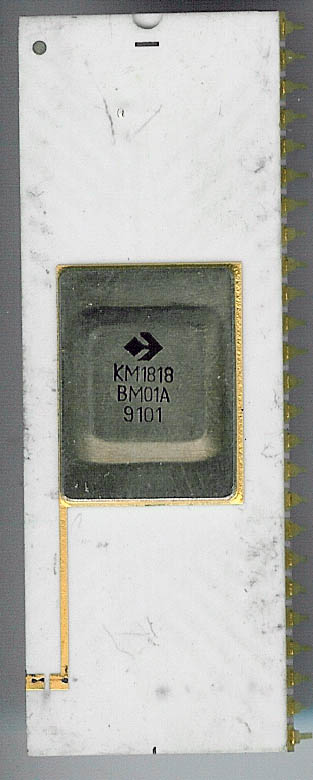
Soviet Electronika KM1818VM01A 8X300 Clone
SMS did not make the SMS300 themselves, they contracted another Silicon Valley company to fabricate them. Signetics, founded in 1961 by ex-Fairchild workers, was the first company founded to solely manufacture ICs rather then discrete transistors. In 1975 Signetics was purchased by Philips but continued to operate under the Signetics trademark until 1993. Signetics made all of the SMS300 devices for SMS, and in 1976 Signetics became a second-source, and could sell the SMS300 under the Signetics brand. By 1978 Signetics had purchased the rights to the SMS300 and renamed it the 8X300. 1977 or 1978 is generally when people think the 8X300 was develped. This is, unfortunately, due to forgotten history as by the time Signetcs bought the design, it had been on the market and in use for over 2 years. Signetics continued to make the 8X300 into the early 1990s where it found wide use in disk controllers, telecommunications and other DSP like environments. The N8X300 was also second sourced by AMD though I have yet to see one. The 8X300 was also *second sourced* by the Soviets in the 80’s and early 90’s by the Electronika state electronics company in what is now Voronezh, Russia. These of course were not licensed copies but they are however, still of interest.

Signetics N8X305N Early 1988
In around 1982 Signetics released the N8X305, the successor to the 8X300. It was functionally compatible but increased the general purpose registers to 13 from 8 among some other instruction improvements that greatly improved upon the data handling deficiencies of the 8X300. Processor speed was also boosted to 10MHz. (200ns instruction time vs 250ns for the 8X300) The N8X305 also used the same pin-out as the 8X300 and the same 50pin DIP package (as well as adding a 68pin PLCC). AMD second-sourced the 305 as the AM29X305. The N8X305 continued to be made into the 1990s and saw use in many military applications as well. Because of this Signetics/Philips could not simply terminate production. They sold production rights to Lansdale Semiconductor Inc., who still offers the N8X305 to this day.

Signetics N8X401I – 1988
In 1986 Signetics again revised the design and released the N8X401. This processor now had a full 32 instruction (including a RETURN instruction allowing the use of subroutines) The N8X401 also added an 8-bit data bus making data handling somewhat simpler but also increasing the package size to a 64 pin DIP. Internal usable registers was increased to 16 and the instruction width was increased to 20-bits. Clock speed remained at 10MHz but it was now fabricated in ECL (Emitter Coupled Logic). This among other improvements, helped to result in a 35% speed boost over the N8X305.

AMD AM29X305DC – N8X305 Second Source – 1985
The N8X401 was not a great success, primarily because of the competition at the time. By 1986 8-bits, even for a DSP, was rapidly becoming out of date, especially with such purpose built DSPs such as the Motorola DSP56000 and the industry standard setting TI TMS320 series.
Thus is the story of one of the most odd processors to come out of the chip boom of the 1970’s (EA 9002, MMI 6701, AMI S2000 et al). There are several other forgotten processors of that era which are also deserving of some remembrance. In time we’ll try to document their history here at the CPU Shack as well.
December 12th, 2010 at 12:43 am
[…] […]
October 5th, 2012 at 1:16 am
[…] wanted. It could be done in CMOS, Bipolar, SoS, GaAs or even ECL. It was designed (like the Signetics 8X300 and the Ferranti F100) with real time processing in mind, similar to what we would call a DSP […]
December 6th, 2012 at 3:56 pm
[…] The 8X300 was a design of the Scientific Micro Systems Inc. SMS300. You can read the entire history here.The only SMS300 I had ever seen was a picture of one in the 1976 issue of Microcomputer Digest (as […]
August 7th, 2014 at 5:56 pm
From about 1983 to 1992, I was the Applications Manager that provided technical support for the 8X305 and 8X401 at Signetics in Sunnyvale. The development and support teams were small and the support software was simplistic by today’s (even then) standards. Two key personnel that should be recognized are Bill Price who came along from SMS to Signetics and Ata Khan, who was the design manager for the 8X401. Both engineers went on to have lengthy and successful technical and management careers. They were fun days. We viewed our chief competition as the bit-slice families, which also had short, fast instruction cycles. As I recall the 8X305 had its heyday in the hard disk drive controller market.
-FYI
JJ
March 16th, 2015 at 2:14 pm
Interesting article. Actually repairing a system now that has this chip in it.
Modicon / Gould (now Schnieder Electric / Telemecanique) manufactured a PLC controller called the 484. Its still used in many places and has been very durable over the years. I’ve got one that has the ceramic N8X300I and one with a N8X305N.
The later being in my test unit.
October 19th, 2018 at 1:49 am
My circuit team designed this processor along with Ken Krossa who was system architect leader . It was at the time intel did its first processor 4004? We took great pride in that it yielded on the first fab cycle and was so large it completely filled the max optical capacity of mask lenses at the time. Critically we used exhaustive circuit simulation to insure functionality and exhaustive artwork inspection to match circuit schematic. Bill Carter who went in to Xilinx worked on it just out of Santa Clara University
SMS at its start designed a 1024 Ram chip and a new epitaxial silicon 2-layer metal process for it. This memory chip was cutting edge and we transferredit to Signetics ( a Corning sister company) in order to focus on the high speed communications system and special processor which utilized the Signtis fab process we created.
December 9th, 2020 at 11:50 am
The 8X300 was used in the Antares Media Converter, in which it served as kind of a universal disk controller. The unit was a full rack with several types of floppy drives, and a PDP11. It converted between various formats as well as physical types of media. Antares was housed in a barn in Lake Elmo Minnesota.
February 1st, 2021 at 9:33 am
I wrote the microcode for all of Western Digital’s 8×30* hard disk controllers. To simplify programming, I wrote my own assembler using macros. With my assembler, I would just once declare the bit position, bit field length, IVL or IVR, and fast IV address of all 8X300 IO devices. With this info, the assembler would automatically generate rotate, mask, shift, IVb, and port. Big time saver.
WD’s first controller to use the 8X300 was the WD1000, WD’s first hard disc controller and an emulator of WD’s future WD1010 chip. We selected the 8×300 because it could read and process parallelized disk headers in real time at 625 Kbytes a second. Our next design was the WD1001 ECC (error correcting code) disc controller. To correct a disc error, a reciprocal 32 bit polynomial was executed in 8X305 firmware, one of my more challenging programming tasks ever. Another 8X305 application of note was the disk controller we designed for the Fortune Systems 32:16, a early 68000 system. The customer required DMA. The 32:16 bus had 16 bit data and 24 bit addressing. DMA controllers of the era typically handled only 8 bit data and 16 bit addressing. I came up with a DMA solution that required no LSI devices nor counters. I had the 8X305 simulate the 24 bit address counters and 8-to-16 bit bus conversion in software with cheap octal latches. The software loop required to update 16 bits of data, update the least significant byte of the address, maintain a word counter, initiate the DMA state machine, and wait for completion was only 8 8X305 instructions or 2 microseconds (us). This was quicker than the disc.
February 5th, 2021 at 6:05 am
Wow
This brings back memories
February 5th, 2021 at 6:08 am
Wow
This brings back memories
November 1st, 2021 at 4:48 pm
Hi Mike,
It’s interesting to hear from the author of the WD1000/1001 firmware. I wrote an 8X300 disassembler and partially reverse-engineered the WD1000 and WD1001 firmware. The disassembler and the firmware are on github:
https://github.com/brouhaha/s8x30x
https://github.com/brouhaha/wd100x
Like you, I didn’t use the offical 8×300 assembly syntax.
December 6th, 2021 at 8:31 am
I have 2. Pieces of signetics products to let go
A Signetics 2650 instructor up. Development
Tool.
And signetics FPLA programmer. 82S100/101
If interested contact me
March 7th, 2022 at 6:05 pm
As a design engineer at Ford Aerospace in Houston, I designed hardware and software/firmware for NASA mission control in the late 70s / early 80s. Three of these designs used the 8X300 or 305. I designed circuits boards, wrote the code, and also wrote my own FORTH-based assembler. I also used the 8×310 interrupt controller chip. We were very impressed with the speed of this processor, especially the one clock-cycle per instruction execution, including the ability to do a read/modify/write on I/O ports in a single clock cycle. Nothing else available at the time could touch it!
April 5th, 2024 at 6:14 am
I used the 8X300, later the 8X305, together with TDC1010 – TRW – 16 Bit x 16 Bit Multiplier/Accumulator to make an FIR filter, actually the fastest DSP in two chips available at that time.